
![design-review:-usb-c-pd-input-for-yaesu-frg7700-[hackaday]](https://i0.wp.com/upmytech.com/wp-content/uploads/2024/05/185479-design-review-usb-c-pd-input-for-yaesu-frg7700-hackaday-scaled.jpg?resize=800%2C445&ssl=1)
Design Review: USB-C PD Input For Yaesu FRG7700 [Hackaday]

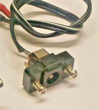
Today is another board from a friend, [treble], who wants to convert a Yaesu FRG7700 radio to USB-C PD power. It’s yet another review that I’ve done privately, and then realized I’ve made more than enough changes to it, to the point that others could learn from this review quite a bit. With our hacker’s consent, I’m now sharing these things with you all, so that we can improve our boards further and further.
In short, this board is a PD trigger. Unlike the usual PD triggers, however, this one is fully configurable, since it has a 32-bit MCU with good software support, plus, the PD PHY is also well known and easily controllable. So, if you want special behavior like charger-power-dependent profile selection for powering a static resistance load, you can implement it easily – or, say, you can do PPS for variable voltage or even lithium ion battery charging! With a bit of extra code, you could even do EPR (28 V = 140 W power) with this board, instantly making it into a pretty advanced PD trigger, beyond the ones available on the market.
Also, the board has some PCB art, and a very handy filter to get some of the USB-C charger noise out. Let’s take a look at all of these!
Current Flow Improvements
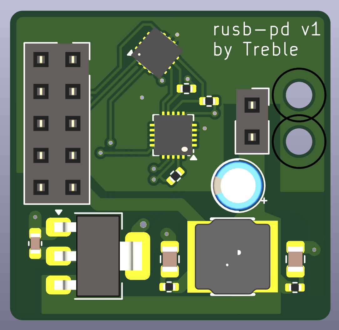
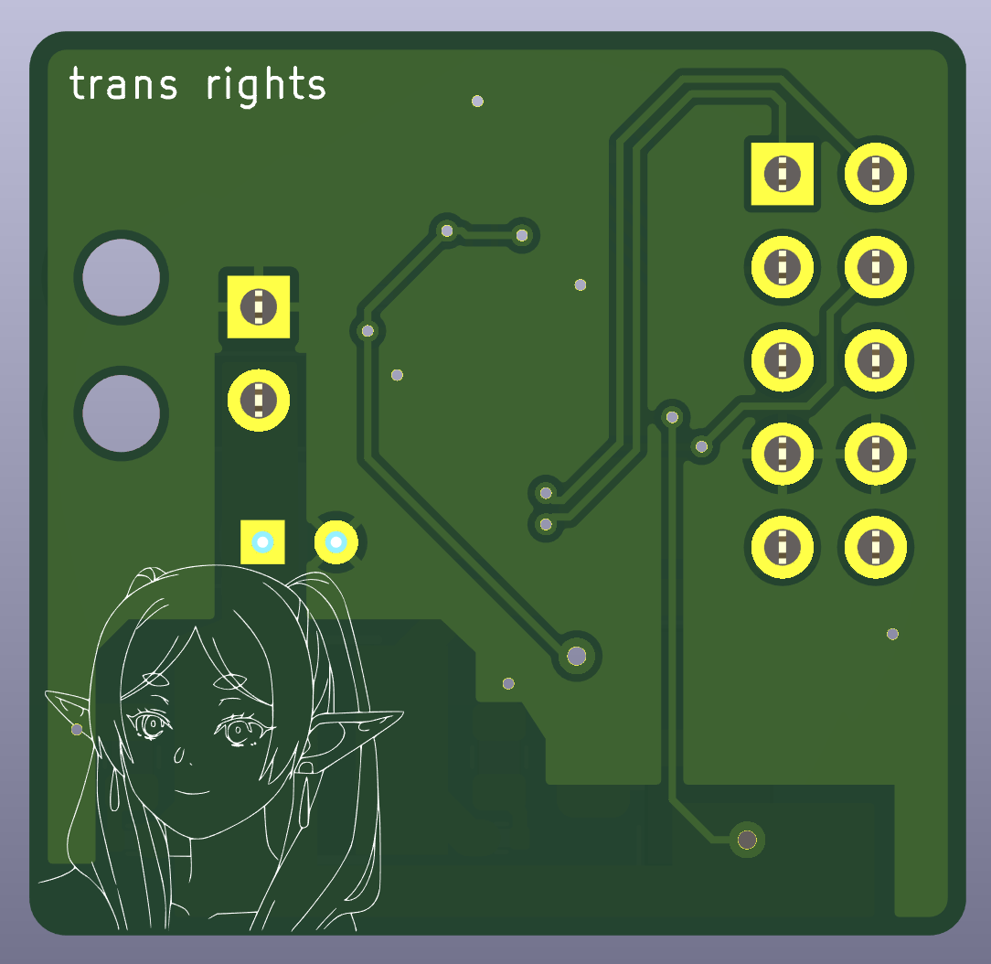
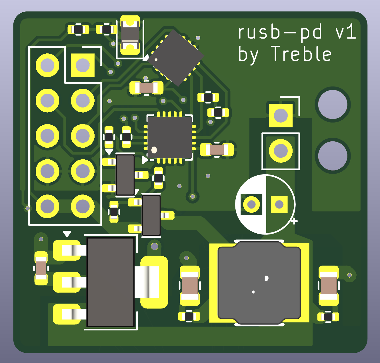
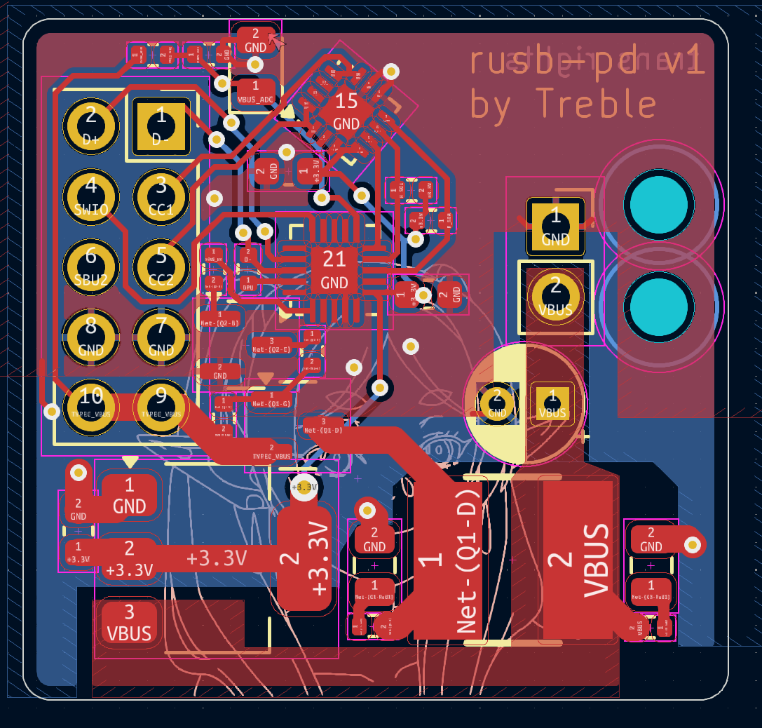
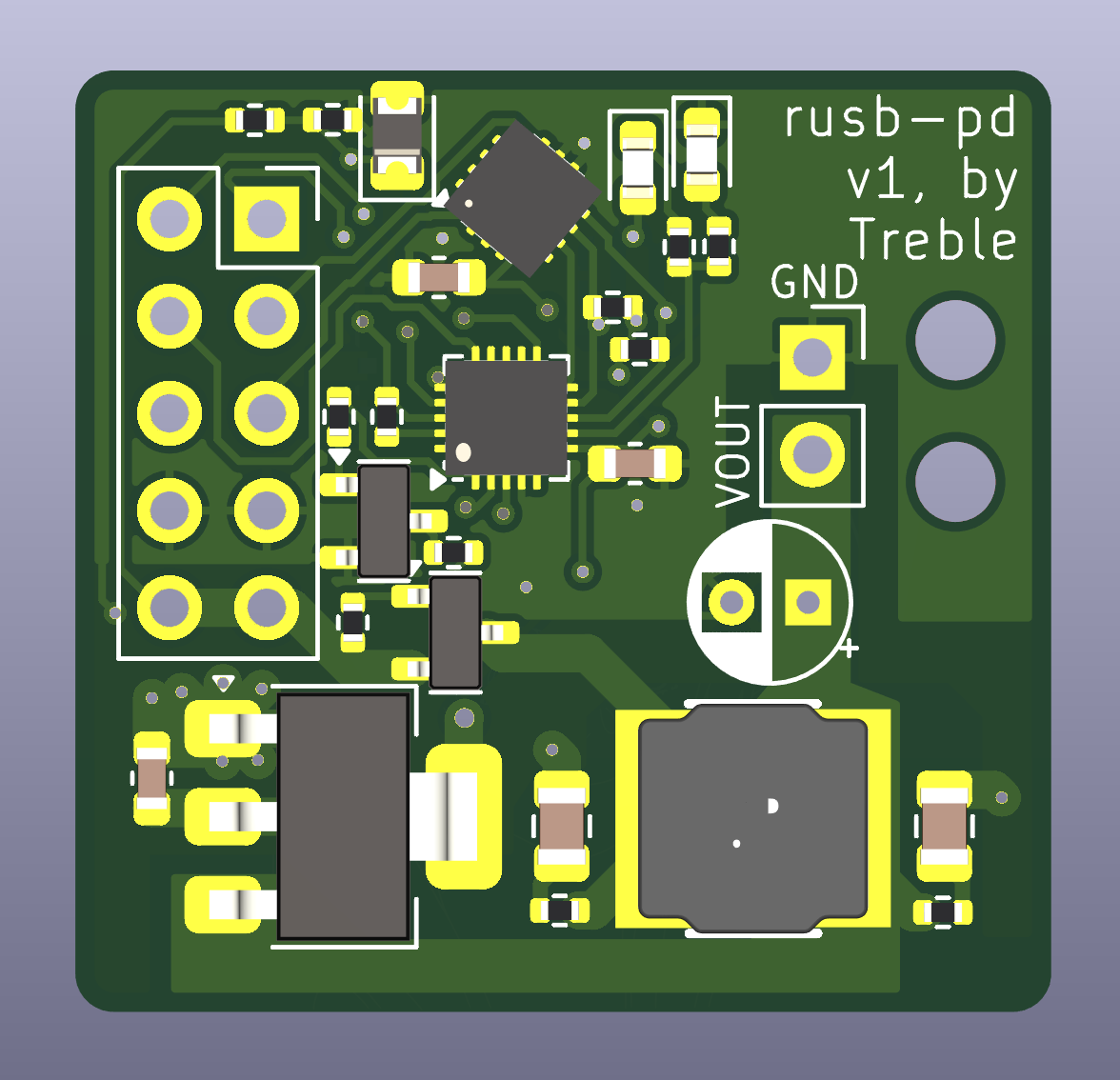
First of all, the back of the PCB has art. This is a problem. Specifically, the art has to be bigger. See, fabs might struggle drawing thin silkscreen lines. So, I will take the liberty of enlarging it. This board is 25×25 mm in size, after all. Due to the way KiCad works, I’ve had to ask for the original .svg file from [treble] for that. Here’s a tip that I myself should follow more, if you’re adding PCB art, storing its sources alongside the board is pretty valuable for whenever it might need to be regenerated or modified!
This board is seriously nice. It has thick traces for power, and, it makes liberal use of filled zones for higher-current tracks, too! It’s not often that I see these fills used, even for higher-power areas, and truth be told, I get lazy to draw them, but they are possibly the cleanest choice for a board that fulfills a power-related purpose. Also, as usual, it’s just two layers, something dear to my heart.
Now, let’s take a good look at the two layers we have. This is a board that current is supposed to flow through, and if you have an eye for it, you might notice that it will be impeded more than you’d want it to be, in ways that are easy to fix.
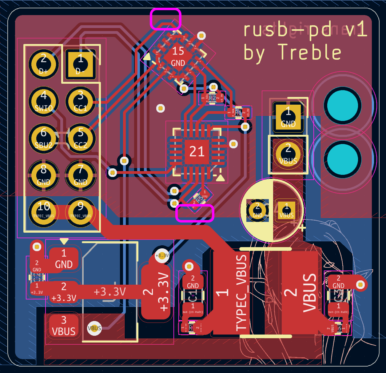
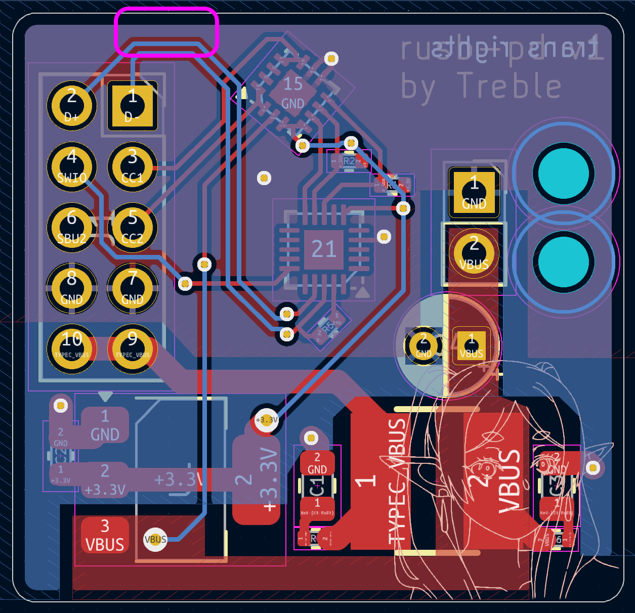
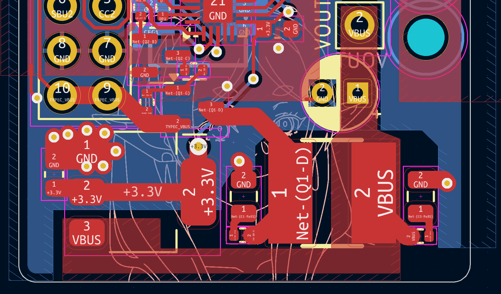
Take a look at the board’s bottom layer. It has a ground plane, yes, but there are also tracks going all across it. If you try and visualize the way that ground return current could flow across the board, you might realize that it has to go through a few small slivers of copper; this is despite the ground fill being present on both sides. Let’s fix this.
Here are three spots where you could straightforwardly add ground connectivity purely by moving vias. I usually look out for such spots as part of my after-design cleanup routine – something I might spend a good half an hour on; just, idly glancing at the board in the 3D viewer, looking here and there, trying to notice any things I could improve upon. Here, if you wanted a high return on your investment, you could move these vias and gain whole two new paths for ground return current to flow through.
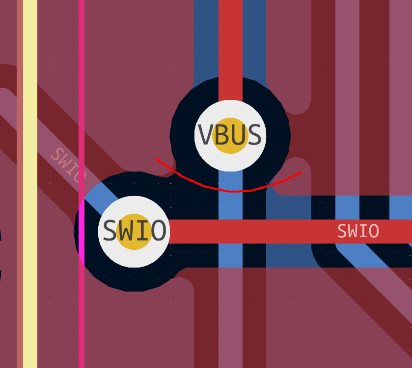
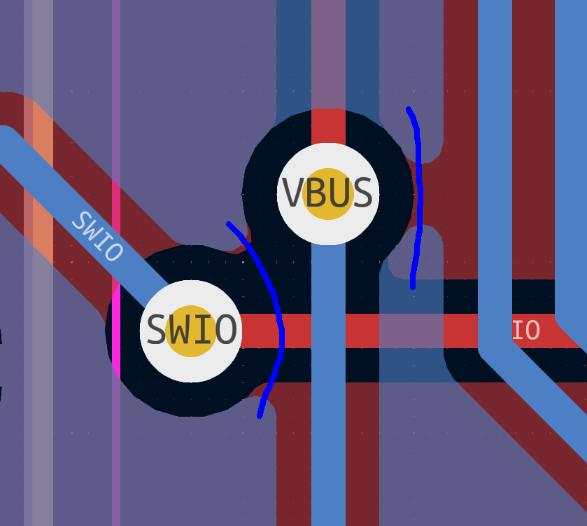
Moving tracks around will yield way bigger returns for freeing up some ground area. For a start, the SWIO pin, wittily wired up to an SBU pin on the USB-C connector with the trace snaking between the 2.54 mm header pads, doesn’t have to go on B.Cu at all. The VBUS connection of the FUSB302 could also be moved to the left edge, all around the 2.54 mm connector, so that it doesn’t have to cut the ground polygon in half. Furthermore, we could improve upon USB diffpair routing by rotating the CH32V003 90 degrees clockwise, and having the pairs go back onto the front layer again at the top. Part of the 3.3 V track could be routed on the top if you rotate a resistor 180 degrees, and voila, we now have a healthy and plentiful ground polygon.
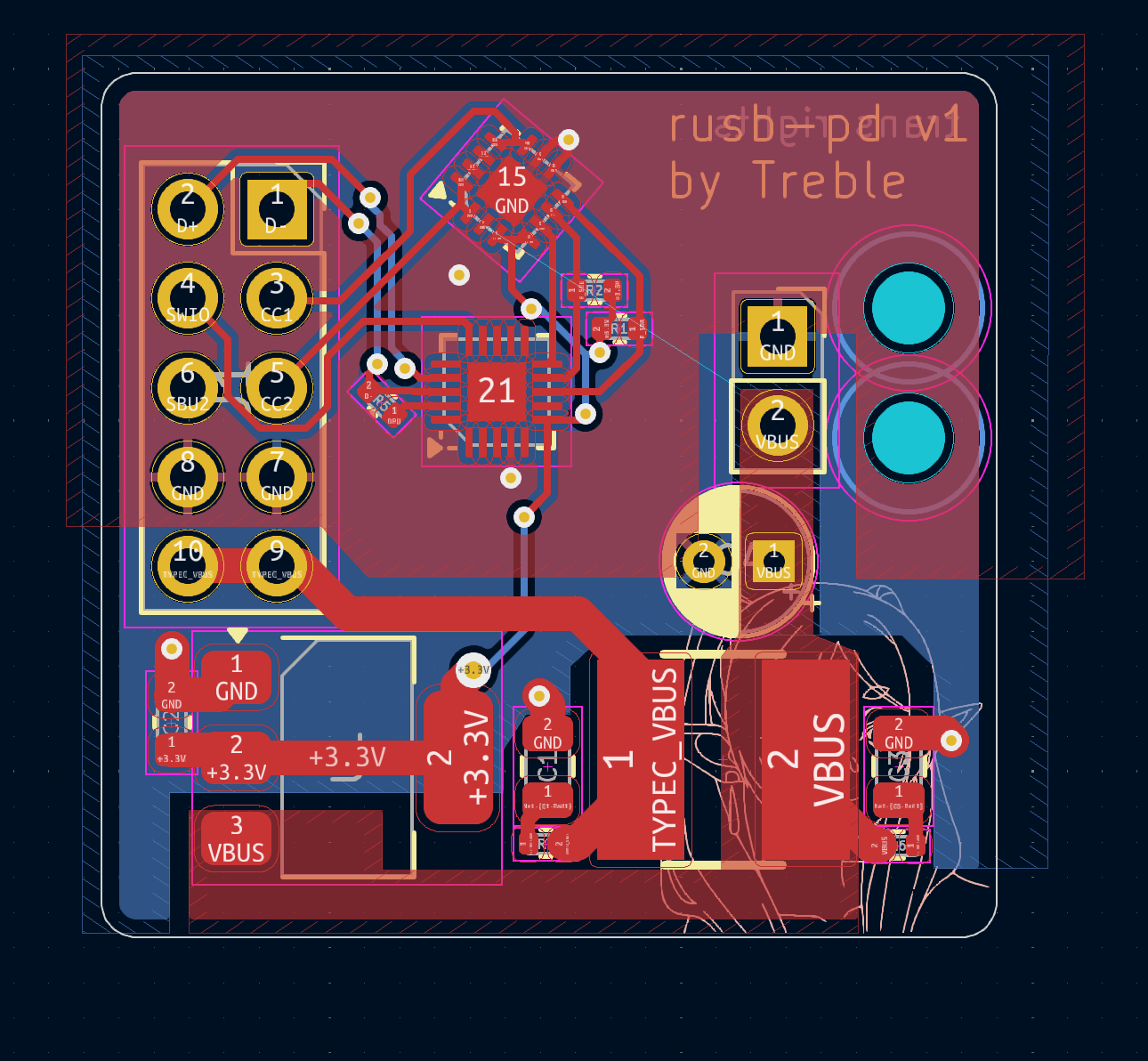
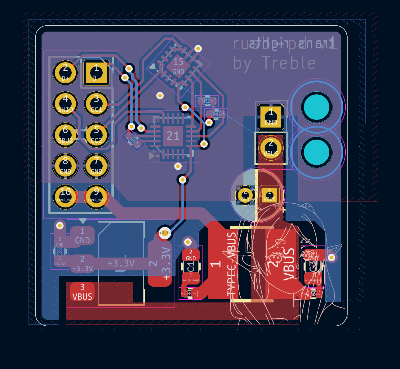
“Route as much of your board on a single layer as humanly possible” is still a great guideline, and it helps here, too. It also helps if you look at your board and visualize the way that ground return current will flow, from one side to the other, all along the signals.
Only a few small details are left. The ICs don’t have decoupling caps on their 3.3 V inputs, and we could easily add them – cleaner power is always a plus. Oh, and the linear regulator could use a couple more vias from its GND pin – purely for the heat dissipation potential. There’s a 1.5 K resistor used for a USB pull-up, and I2C uses 3.3 K pullups in the same package – I’ve changed them to use 1.5 K too, just as a BOM optimization reminder; should work wonders for I2C.
Implementation Details And Polish
Something I don’t expect hackers to know but is nice to keep in mind – the VBUS pin of the FUSB302 is fault-prone and PSU noise on it can cause the FUSB to die in a way that short-circuits the 3.3 V rail, to the point that the Pinecil soldering iron eventually disconnected it in a new hardware revision, and the community has developed guides to disconnect the VBUS pin. Furthermore, the VBUS connection on the FUSB is not even needed for any part of the PD process; essentially, it’s not even a nice-to-have, all you get is an interrupt that doesn’t carry any meaning in our “bus-powered” arrangement. Let’s disconnect it – that frees up quite a bit of ground and routing space around the FUSB302.
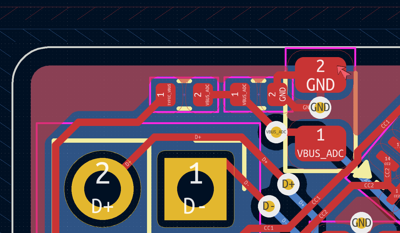
What else? Here’s something to consider – the radio might not be happy with 5 volts on its power input, which is an inevitability given how the USB-C negotiation process works. Remember, first, you get 5 V, and then you have to negotiate further up. This is why PD trigger ICs tend have a PG pin, that you can connect to a P-FET gate, and that pin is only driven after a successful negotiation. In our case, we have MCU GPIOs we can use instead!
For that to work, let’s rewire the VBUS on this board. The MCU and its 3.3 V linear regulator can be powered from the raw USB-C input, we won’t gate them with the FET, of course, that’d lead to a chicken and egg problem. It makes sense to power the Pi filter through the FET, though – mostly because we have some board space between the USB-C input and the Pi filter, where a SOT-23 FET could very nicely fit. The radio could consume as much as 3 A at 12 V; at least, that’d be the maximum capability of a typical USB-C PSU you could use with this board. My FET of choice, then, is AO3401 – a classic FET that works at 30 V 4 A, and will even let this board be a pretty generic trigger board if needed, and; higher current, you can stack one more SOT23 FET on top.
With an NPN driver and a provisional 3:1 divider for the gate voltage, the “power good” circuit fits into the board space wonderfully. If it’s not needed, it can be easily jumpered with a 0 R resistor across the FET pads, but adding this circuit retrospectively would be bothersome – it helps that we have the footprints for it. Remember, traces and footprints are free to add, fundamentally – just like silkscreen markings.
How Will You Use Your Board?
Another great thing to visualize is – after you assemble your board, how will you interact with it? Here, [treble] still has to write the USB-PD firmware – in C++, no less, my MicroPython stack won’t be directly applicable, as much as I will help, but [Ralim]’s open-source PD stack used in the Pinecil could work wonderfully! While integrating that, she will have to debug things. Possibly, might even have to debug it some more later on, with the board installed into the radio chassis. It’s a project one hacker could pull off without a doubt, and, there’s things you could add to your board that will help.
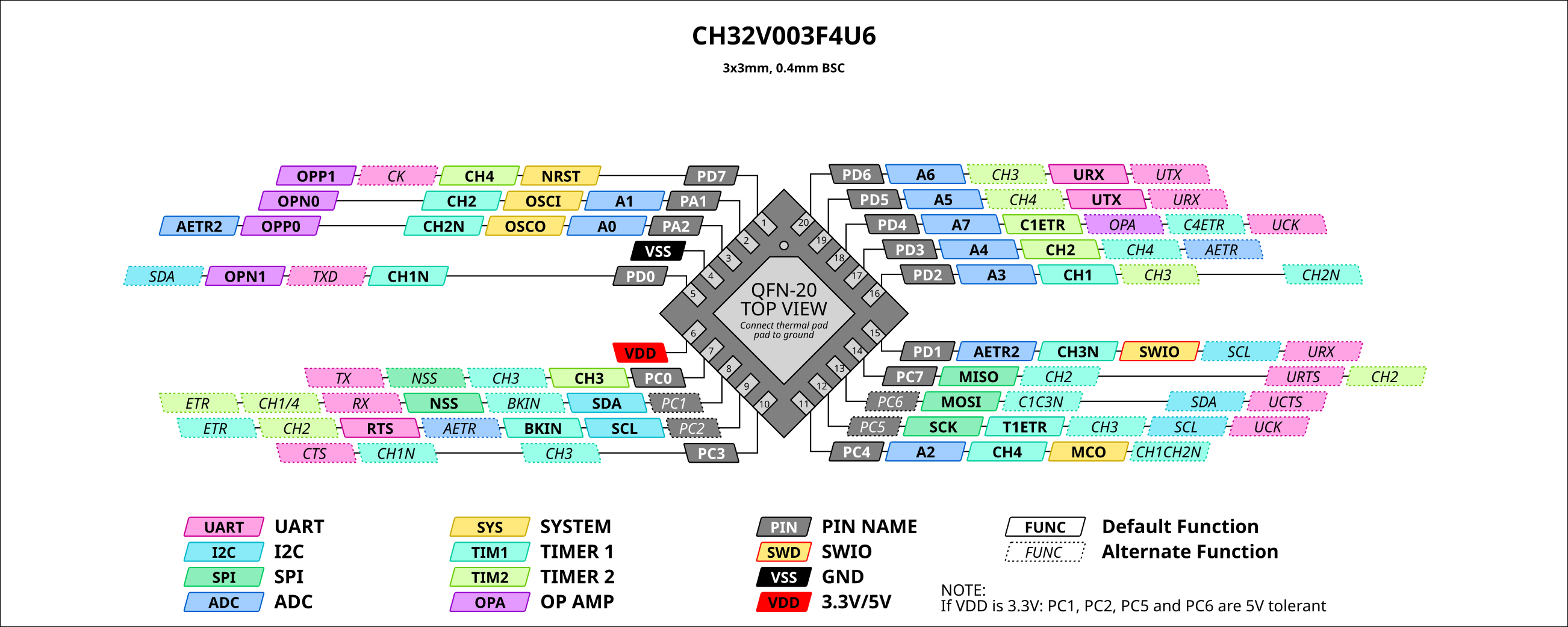
The SWIO pin of the CH32V003 goes to an SBU pin on the USB-C socket. This is a great decision, because you can easily reflash the MCU without disassembling the entire radio – just have a USB-C plug with SBU exposed and that’s enough. Also, when I’m thinking about it, it might be troublesome during active development, because [treble] will have to constantly unplug and plug the PSU and the programming plug while debugging the in-progress firmware. Now, she could solder to the 2.54 mm pin headers, sure – alternatively, you could add an extra SWIO header at the edge and make her job a bit easier. I can’t find much space for it, sadly, so I suppose a female header with longer male pins (Arduino and Wemos shield style) can do just as well, also allowing to probe CC pins as a bonus.
I feel like there’s a good few more things you can add to improve development and usage comfort. Will there be a failure mode where the board has to signal to the user that something’s gone wrong – say, with a 5 V USB-C PSU inserted? Let’s add two LEDs on one pin – could even do WS2812 sometime later. What about I2C communications, what if tapping them would be useful during the board’s development? Let’s add a QWIIC socket and pull the I2C lines onto it – not for expansions, but rather, so that you have a socket you can easily wire up to a logic analyzer, plug it in and unplug it at any point.
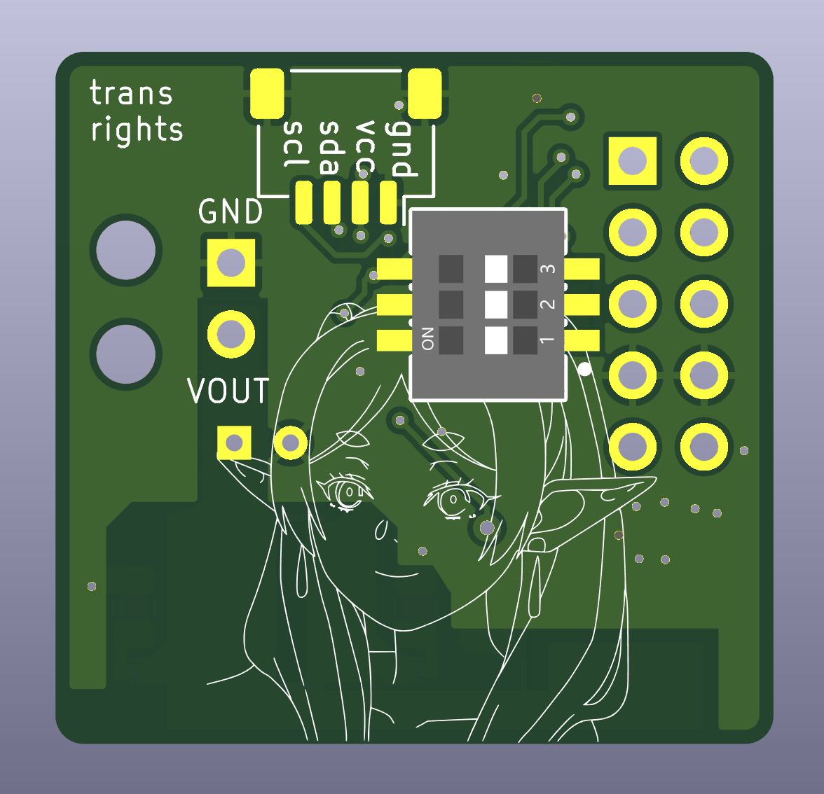
There’s some arguments to be made for breaking out as many CH32V003 pins as possible. I will refrain from it, as much as it’s tempting – at this point, there isn’t a lot of board space in the spots where it matters. It would be cool to have them on testpoints though! Speaking about that, I’ve just realized – you could add a tiny SMD three-position DIP switch onto the back of the board reasonably easily, so that you can have “profiles” for the trigger board, CH224 PD trigger board style. I’ve found the tiniest three-position SMD DIP switch that LCSC has, then added it to the back of the board, trying to still have the ground fill as intact as possible – the idea is that this is a nice feature for whenever the board might be used as a more general-purpose trigger board. When not populated, it serves as a breakout for three ADC-capable GPIOs, GND, and 3.3 V!
Now, I’d like to emphasize: the DIP switch is not exactly necessary in this project. It falls into “something that’d be cool to fit in space left over, if the board is to be used in an entirely different setting”. Overall, I try not to push features this remote onto people while doing design review – plus, it does clash with the silkscreen. So, this addition is easily removable from the PCB files, and it doesn’t have to be populated either. Also, I’ll stop the additions here, to avoid feature creep.
That about wraps it up for things I feel like this board needs. Let’s talk about an aspect where I’d like your opinion.
Questions For The Audience
Now, here’s a question for the audience, on two things I’m not well-versed on. First one is – here’s a Pi filter. The purpose is filtering out 300 KHz USB-C charger switching frequency that [treble] has noticed being produced by a USB-C charger she’s picked. Having simulated this filter in LTSpice, it appears to be good for filtering out 200 KHz and above. Does that look correct? And, any things she should look out for when it comes to component choices?
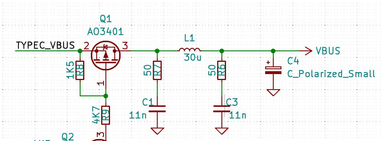
Another question is – the ground cutout under the Pi filter. My understanding is – the more ground, all over the board, the better. [treble] decided to remove ground under the Pi filter, as far as I recall, due to a gut feeling that it’d decrease noise imposed by the inductor. Does that make sense? I’m tempted to say “no”, but I can’t formulate a good enough explanation on the specific downsides and how it might need, which is why I’m asking you.
Another board reviewed, and due to the way it’s built, I can easily imagine ordering a dozen for use in my own projects – thanks to [treble] for sharing this, and I hope this feedback helps! As usual, if you would like a design review for your board, submit a tip to us with [design review] in the title, linking to your board files. KiCad design files strongly preferred, both repository-stored files (GitHub/GitLab/etc) and shady Google Drive/Dropbox/etc .zip links are accepted.
I thank [Julianna] for helping me check the the CH32V003 circuit!