KiCad 8 Makes Your Life Better Without Caveats [Hackaday]

A few days ago, KiCad 8 was released, and it’s a straight upgrade to any PCB designer’s quality of life. There’s a blog post as usual, and, this year, there’s also a FOSDEM talk from [Wayne Stambaugh] talking about the changes that we now all get to benefit from. Having gone through both of these, our impression is that KiCad 8 developers went over the entire suite, asking: “this is cool, but could we make it better”? The end result is indeed a massive improvement in a thousand different ways, from small to fundamental, and all of them seem to be direct upgrades from the KiCad 7 experience.
For a start, KiCad works better with whatever other tools you might use. There’s the recently added LTSpice schematic import and overall serious SPICE simulation improvements, SVG and DXF import for the schematic editor, an “export copper” option for STEP, mechanical CAD import QoL tweaks, IPC-2581 export for whenever manufacturers start supporting it, and Cadence Allegro netlist export in case you’d like to use KiCad for schematic duty only. You can now also import footprint and symbol libraries from Altium and CADSTAR, as well as import EasyEDA projects directly, and this release brings enough features that you might just want to try those importers out.

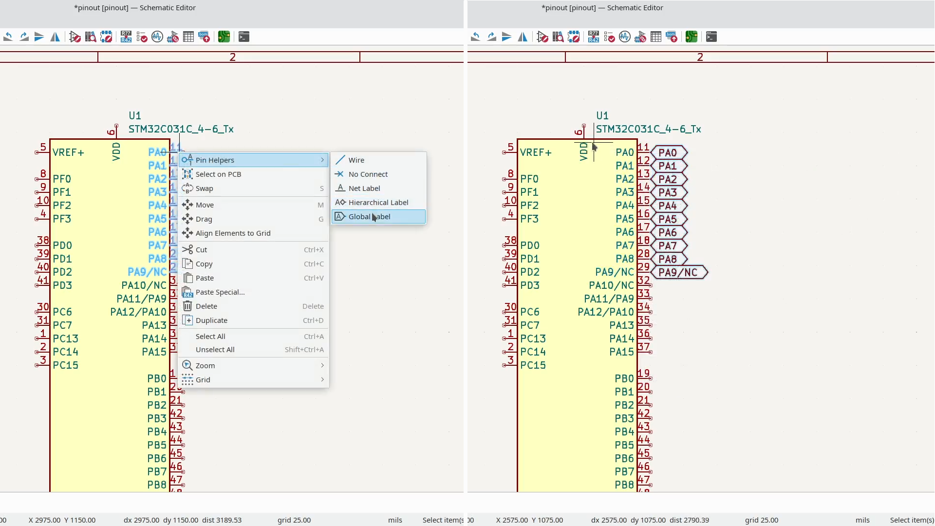
A lot of sharp edges have been filleted in on the PCB editor front, too. You can now resize length tuning patterns on the fly, easily assign nets to graphic shapes to aid your RF or capacitive touch design, power symbols now have editable names, and there’s a new pin 1 marker on the block that should work better in more situations than the previous convention ever could. For automation afficionados, we’ve seen kicad_cli introduced in KiCad 7, and now it adds ERC/DRC exports for all your automated pull request review needs, BoM export, gITF and VRML 3D model exports, and a bunch more.
KiCad’s usage is ramping up, and industry players are taking note – for instance, Wurth Electronics has recently pledged to bring all their components to KiCad as a library. On the KiCad 9 roadmap, we see stable API IPC interface for Python scripts, visual diff and merge for Git, license embedding into files, reusable schematics and design blocks, pad stacks and guard rings, ODB++ export, certainly, quite a bit more that we didn’t yet know we needed. Oh, and they don’t forget about keeping things up to date either – this release brings a trove of documentation and UI translation updates.
Whatever your toolkit is, chances are, KiCad 8 works with it way better now, and whatever kind of KiCad user you are, there’s something in this release for you. Consider trying KiCad 8 out, report bugs if needed, donate, or maybe even get some KiCad merch while at it. It is wise to hold off on a .0.0 release, but all the new features sure make it a tempting offer.

![kicad-8-makes-your-life-better-without-caveats-[hackaday]](https://i0.wp.com/upmytech.com/wp-content/uploads/2024/02/170269-kicad-8-makes-your-life-better-without-caveats-hackaday.png?resize=800%2C445&ssl=1)