
![watch-sls-3d-printed-parts-become-printed-circuits-[hackaday]](https://i0.wp.com/upmytech.com/wp-content/uploads/2024/06/190795-watch-sls-3d-printed-parts-become-printed-circuits-hackaday.png?resize=800%2C445&ssl=1)
Watch SLS 3D Printed Parts Become Printed Circuits [Hackaday]
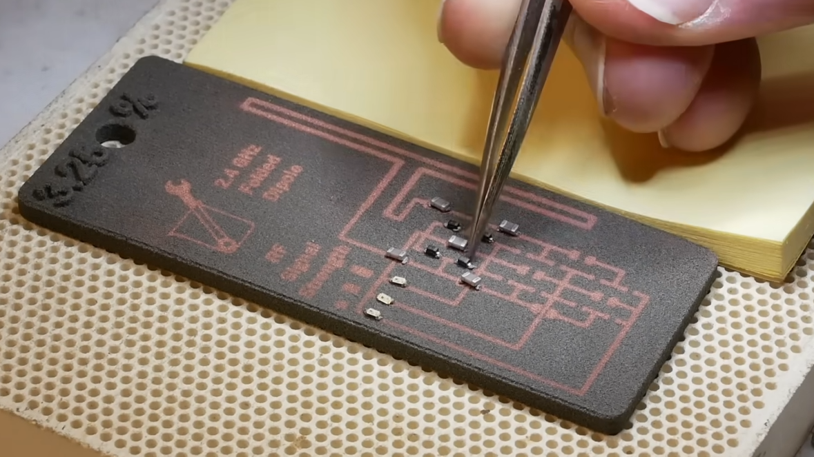
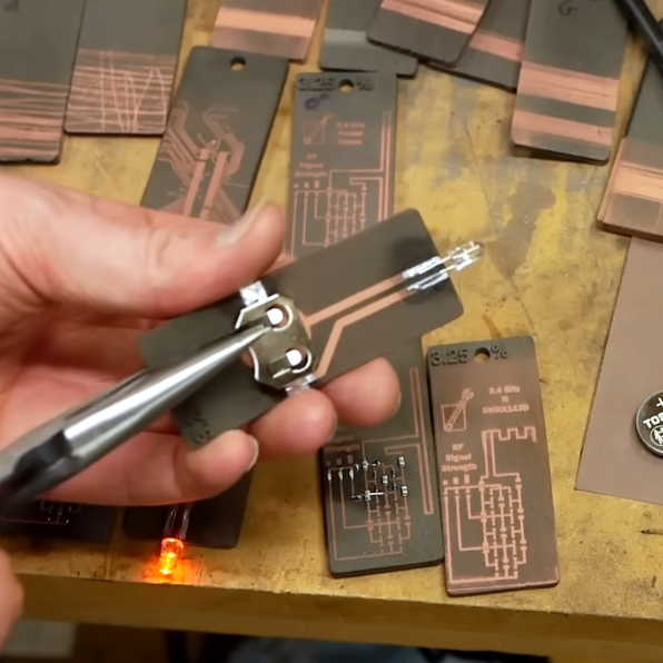
[Ben Krasnow] of the Applied Science channel recently released a video demonstrating his process for getting copper-plated traces reliably embedded into sintered nylon powder (SLS) 3D printed parts, and shows off a variety of small test boards with traces for functional circuits embedded directly into them.
Here’s how it works: The SLS 3D printer uses a laser to fuse powdered nylon together layer by layer to make a plastic part. But to the nylon powder, [Ben] has added a small amount of a specific catalyst (copper chromite), so that prints contains this catalyst. Copper chromite is pretty much inert until it gets hit by a laser, but not the same kind of laser that sinters the nylon powder. That means after the object is 3D printed, the object is mostly nylon with a small amount of (inert) copper chromite mixed in. That sets the stage for what comes next.
Activating the copper chromite is all about dumping enough energy into the particles, and that gets done with a pulsed laser. This is how the traces are “drawn” onto the printed object, and these traces will be copper-clad in the next step.
Once the copper chromite catalyst is activated by the second laser, the whole 3D printed object is put into a chemical bath for electroless copper plating. Again, only the places hit by the pulsed laser end up plated. Places not hit by the second laser remain inert.
There’s an interesting side note here. Electroless copper plating is a well understood process used by every PCB manufacturer in the world. But the recipes are all proprietary and [Ben] tried without success to mix up an effective batch. In the end, a talk with OpenAI’s ChatGPT helped crack the case by suggesting a procedure that worked, saving [Ben] a ton of time. Skip to 8:10 in the video if you want to know all about that.
The result is a 3D printed nylon object into which solder-able copper traces are well and truly embedded. The test pieces work out great, but even better, there’s no reason the objects and traces even have to be planar. All it would take is a pulsed laser able to focus on a curved surface in order to create curved traces on a 3-dimensional part.
We’ve seen copper-plated 3D printed PCBs before, but this is something very different and really elegant. The whole workflow has a lot of moving parts, but once controlled it’s remarkable repeatable.
[Ben] has actually tried putting copper traces on SLS printed parts before, but with only limited success. Recent advances in technology and tools have really made the process sing. Watch it all in action in the video, embedded below.