
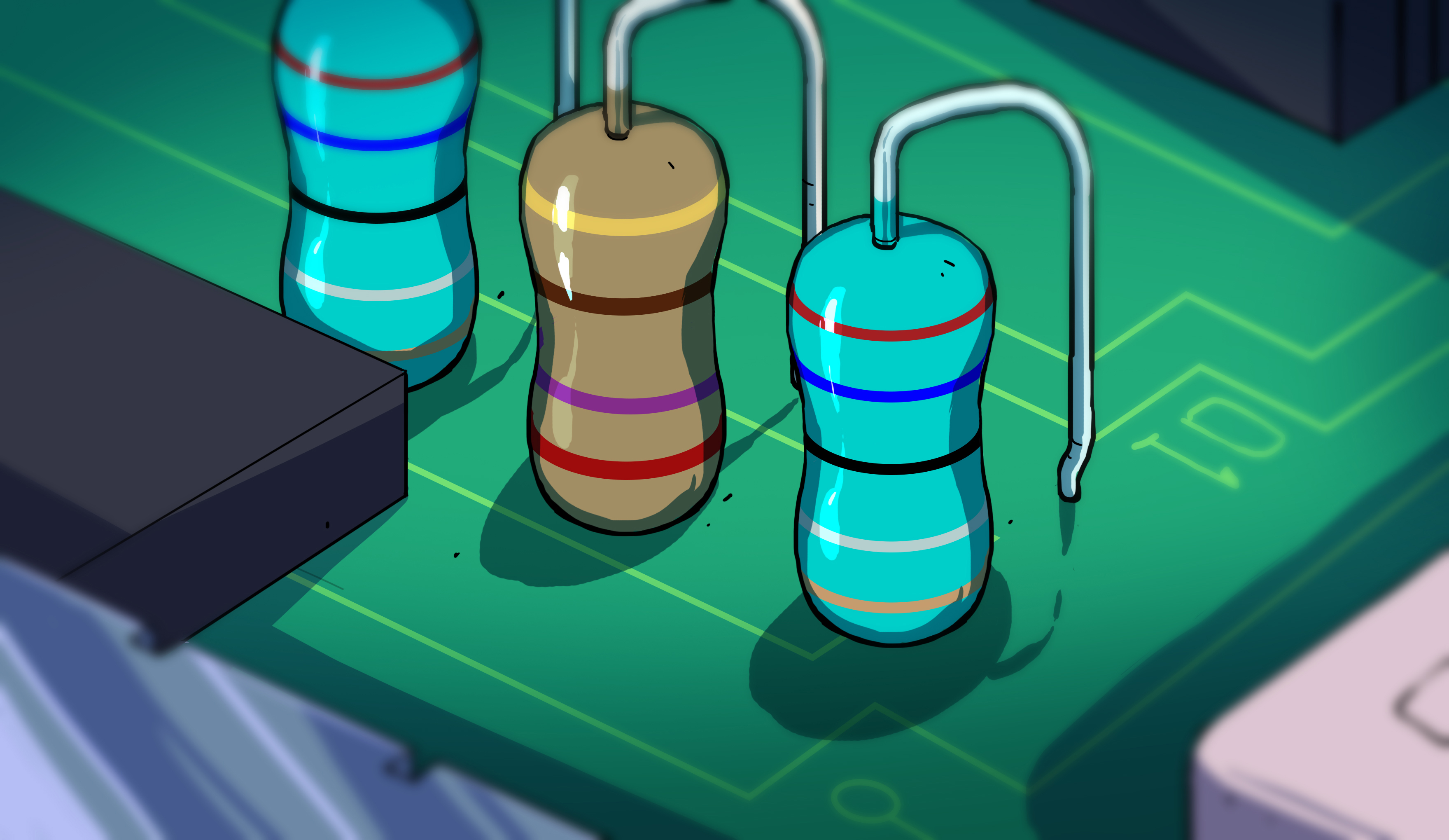
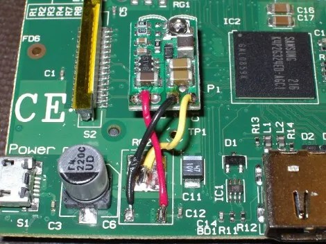
![switching-regulator-layout-for-dummies-[hackaday]](https://i0.wp.com/upmytech.com/wp-content/uploads/2024/06/188825-switching-regulator-layout-for-dummies-hackaday-scaled.jpg?resize=800%2C445&ssl=1)
Switching Regulator Layout For Dummies [Hackaday]
Last time, we went over switching regulator basics – why they’re wonderful, how do you find a switching regulator chip for your purpose, and how to easily pick an inductor for one. Your datasheet should also tell you about layout requirements. However, it might not, or you might want to deviate from them – let’s go more in-depth on what those requirements are about.
Appreciate The Feedback

There’s a few different switching regulator topologies. Depending on your regulator’s topology and how many components your chip contains, you might need some external components – maybe a Schottky diode, maybe a FET, or maybe even a FET pair. It’s often that the FET is built-in, and same goes for diodes, but with higher-current regulator (2 A to 3 A and above), it’s not uncommon to require an external one. For sizing up those, you’ll want to refer to the datasheet or existing boards.
Another thing is input and output capacitors – don’t skimp on those, because some regulators are seriously sensitive to the amount of capacitance they’re operating with. Furthermore, if you fail to consider things like capacitance dropping with voltage, you might make your regulator very unhappy – not that a linear regulator would be happy either, to be clear. We’ve covered an explainer on this recently – do check it out!
One thing you will likely need, is a feedback resistor divider – unless your switching regulator is pre-set for a certain voltage or is digitally controlled, you need to somehow point it to the right voltage, in an analog way. Quite a few switching regulators are set for a certain voltage output, but most of them aren’t, and they will want you to add a resistor divider to know what to output. There’s usually a formula for resistor divider calculation, so, pick a common resistor value, put it in as one of the resistors into the formula, get the other resistor value out of that formula, and see what’s the closest value you can actually buy. Don’t go below about 10 kΩ so that you don’t have unnecessary idle power consumption, but also don’t go too far above 100 kΩ to ensure good stability of the circuit.
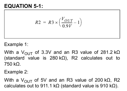
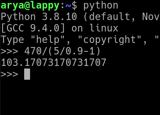
Some datasheets might even have a table of pre-calculated values for you to use. In that table, they might call for a very specific resistor value, but you usually can tweak that for the cases where all of your components have enough leeway. Would you care if your output was 5.1 V as opposed to 5.0 V, or 3.5 V instead of 3.3 V? Usually, you wouldn’t, and it might even be a little better if you increase the voltage a tad, so feel free to substitute that 157 kΩ resistor for a 160 kΩ one – just run the datasheet formula calculations to make sure you know what you will actually get.
Respect The Layout
It’s not always that you have a layout example picture in the datasheet. For instance, it could be that you simply get a list of requirements for the layout, or even no requirements at all – sometimes you’ll just be reverse-engineering a board. Even if your datasheet is pretty good, sometimes, you will feel like deviating from the datasheet-provided example pictures. Here are some guidelines to know how to layout things safely.
For a start, when it comes to placement of the feedback resistors, you’ll want to put them both as close as possible to the FB pin – the midpoint connection between them (the FB-connected track) is the sensitive part, since it’s high-impedance. So, the FB connection ought to be very short, and, of course, the GND connection has to be good – having a via to the GND polygon at the FB-GND resistor is a good idea. On the other hand, it’s okay to pull the VOUT connection for the feedback divider on the opposite layer through vias, because that is a low-impedance connection and it’s less sensitive to noise. If feasible, connect the VOUT connection “after” the capacitors, too, so that it isn’t measuring the point between the inductor and the capacitors, where current flows back and forth.
It pays to ensure that there’s uninterrupted ground on the layer directly under your regulator, as clean as possible, save for maybe that VOUT track, but even that can be worth routing out of the way. Switching happens at high frequencies, anywhere from 100 kHz to 2 MHz, your regulator datasheet will say which,, and it’s a noisy process. Anything less than a full and accessible ground polygon under the switching areas can, in the worst case, turn your regulator into a full-on noise problem in your circuit.
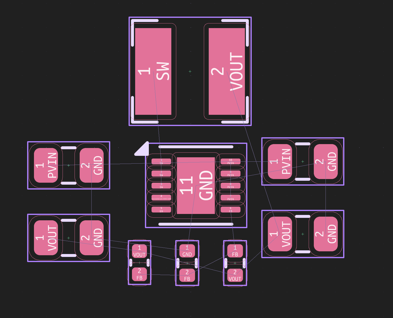
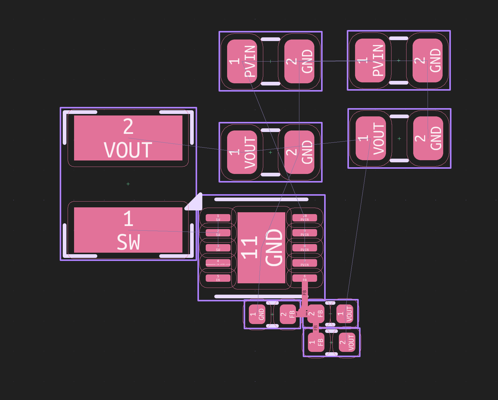
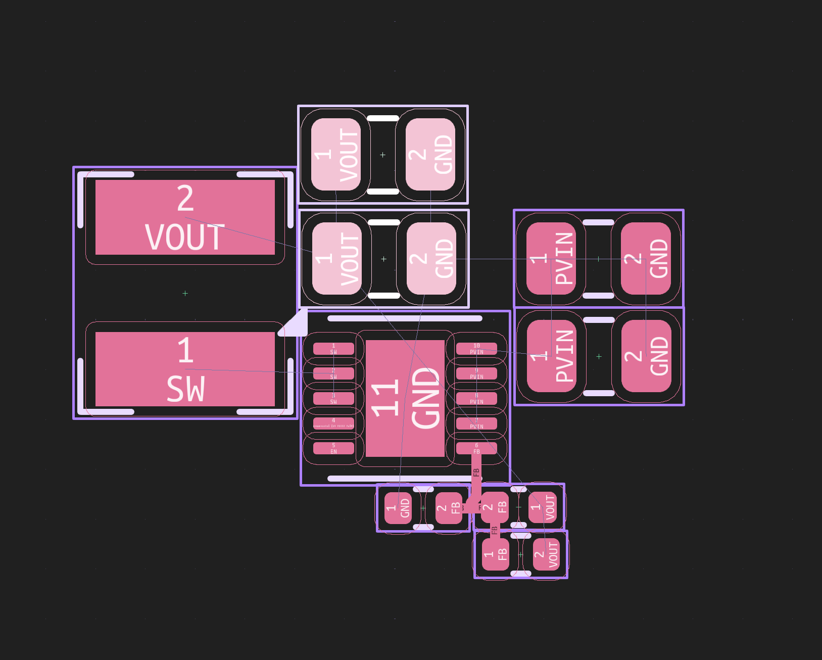
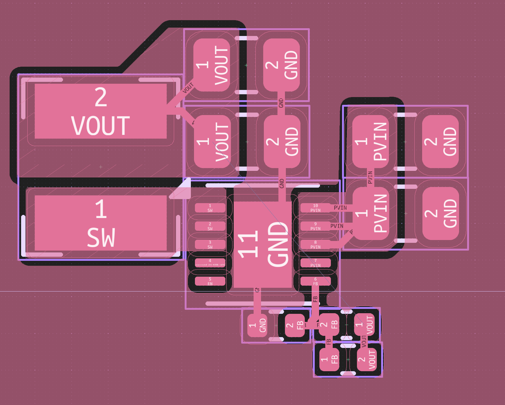
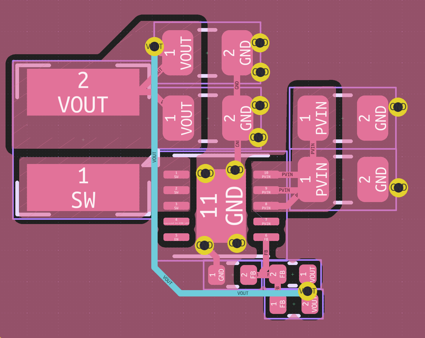
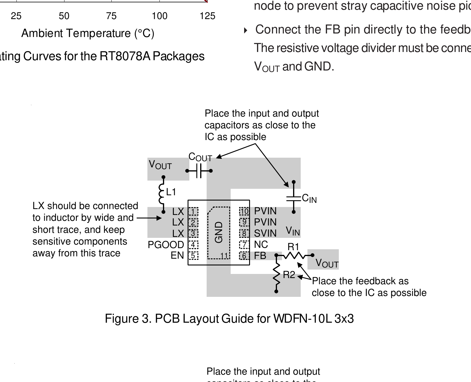
If your regulator has an ‘analog’ ground pad, respect that, and see what the datasheet says – the usual rule is to keep it away from the area where switching happens. Oh, and, it’s often that you need a ground fill directly under the regulator, on the same layer, too – for any switching that happens, whether it’s an internal FET and/or diode, or a driver for external FET gates. You can still try and protoboard a switching regulator circuit, but you’ll want to follow the next layout rule at the very least.
It’s important to put your inductor, diodes and all other components like capacitors as close to the switching regulator chip as you can. With current flowing through them at high frequencies, the connections between them can all become antennas, and the tighter you bundle all the components together, the smaller that antenna is – inducing less noise onto your circuit, which might interfere with WiFi or other wireless operation, analog measurements, or create weird faults in digital logic. Again, this is for you to mind in case there’s no layout recommendation – most often, there is one somewhere in the datasheet, so look out for it! As for traces, you want to provide a connection that’s as straightforward as possible. On connections where actual switching happens (the SW/LX connection from the chip to the inductor), use planes instead of tracks wherever you can.
In general, switching regulators are a bit of a noise source, so keep them away from analog parts; specifically, the SW/LX inductor-connected side. That’s not to say you can’t use switching regulators for anything where you do analog – a ton of modern microcontroller boards and circuits are using small switching regulators, including the Pi Pico. There will still be a bit of noise on the output compared to linear regulators, so if you want a low-noise rail in some part of your project, say, analog supply voltage for sensitive measurements, you can usually add a low-power linear regulator, or use a Pi filter, or combine both. Also, if you need to get plenty of low-noise 3.3V from a high voltage like 20V, you can also do conversion from 20V to 5V with a switching regulator, and then get 3.3V out of 5V with a linear regulator.
Having assembled your board, do you notice your regulator making audible noise? It’s usually not the inductor itself that’s to blame, since switching regulator frequencies are kept pretty high. More often, it appears that either the regulator’s duty cycle, or the capacitors are at fault, specifically, MLCCs, and the way they interact with your output load. It’s not an uncommon problem, though – here’s a page from Murata that tries to sell fancier “quiet” capacitors to you, a fun appnote from TI, and a PDF from Monolithic Power that suggests you treat your PCB as a musical instrument.
Make The World Go Round
It also pays to learn a bit how switching regulators work in principle, and, you can have some fun with the concept! Whether that’s making a switching regulator out of an opamp, using an ATTiny to do switching regulator duty, or repurposing the ubiquitous $1 switching regulator modules into negative rail power supplies, knowing the inner workings of a switching regulator makes your toolkit all that more rich. All in all, while a switching regulator might need a few more components, the extra effort is one hundred percent worth it, and if you have never added a switching regulator to your board before, your next design might be a good place to start!
Next time, let’s get down to business – pick a few switching regulators for common purposes, then pick components and do layout for a good few regulators at once, all done in an open-source design. After all, a picture speaks a thousand words, and I’ll make sure there are plenty of those.