
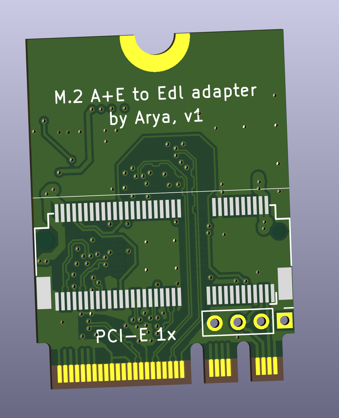
![pcie-for-hackers:-our-m.2-card-is-done-[hackaday]](https://i0.wp.com/upmytech.com/wp-content/uploads/2023/07/134521-pcie-for-hackers-our-m-2-card-is-done-hackaday-scaled.jpg?resize=800%2C445&ssl=1)
PCIe For Hackers: Our M.2 Card Is Done [Hackaday]
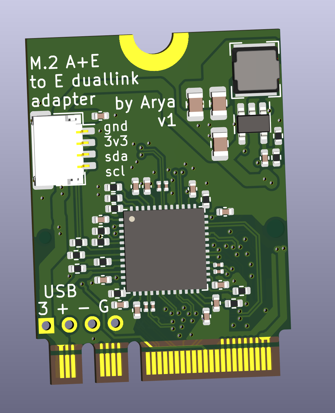
We’ve started designing a PCIe card last week, an adapter from M.2 E-key to E-key, that adds an extra link to the E-key slot it carries – useful for fully utilizing a few rare but fancy E-key cards. By now, the schematic is done, the component placement has been figured out, and we only need to route the differential pairs – should be simple, right? Buckle up.
Getting Diffpairs Done
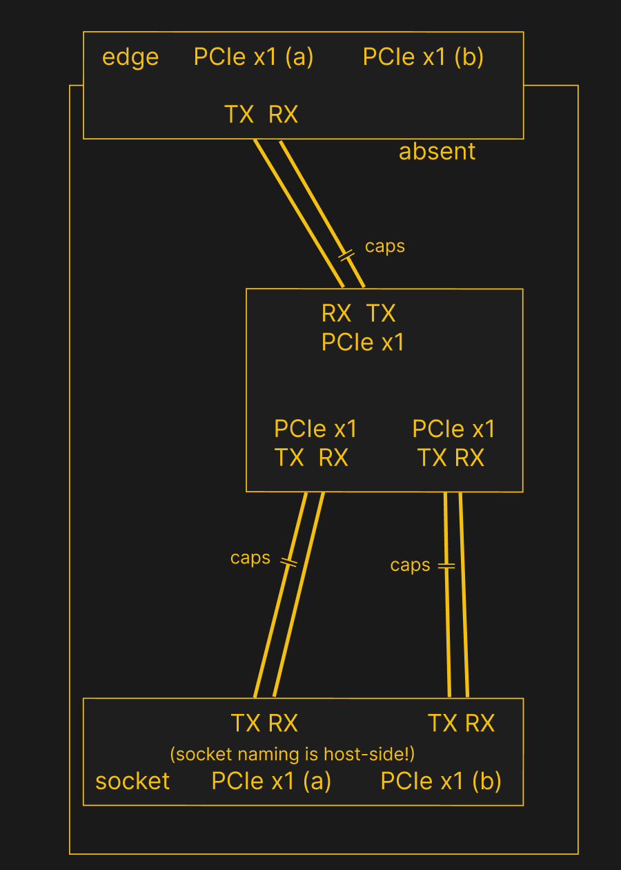
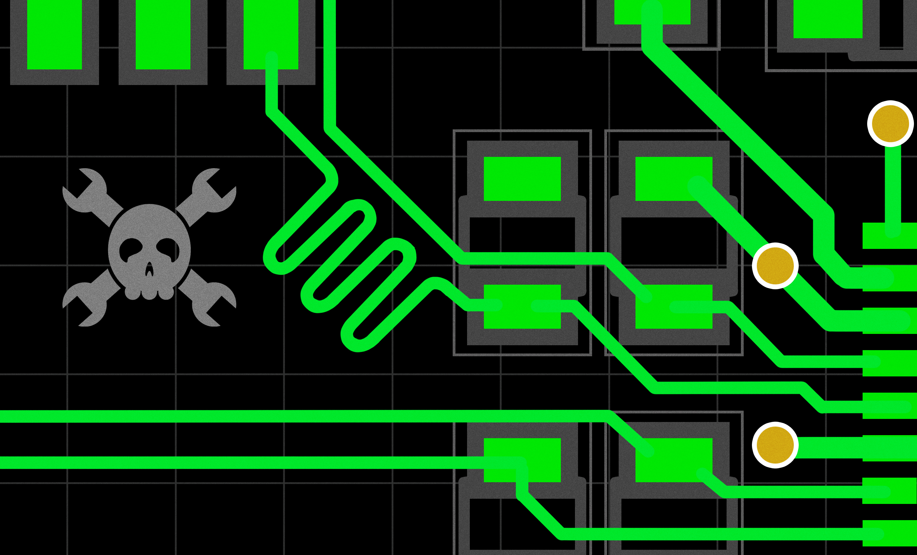
While initially routing this board, I absolutely forgot about one more important thing for PCIe – series capacitors on every data pair, on the host TX side of the link. We need three capacitor pairs here – on TX of the PCIe switch uplink, and two pairs on TX side of the switch – again, naming is host-side. I only remembered this after having finished routing all the diffpairs, and, after a bit of deliberation, I decided that this is my chance to try 0201 capacitors. For that, I took the footprints from [Christoph]‘s wonderful project, called “Effect of moon phase on tombstoning” – with such a name, these footprints have got to be good.
We’ve talked about differential pair calculations before in one of the PCIe articles, and there was a demo video too! That said, let’s repeat the calculations on this one – I’ll show how to get from “PCB fab website information” to “proper width and clearance diffpairs”, with a few fun shortcuts. Our setup is, once again, having signals on outer layers, referenced to the ground layer right below them. I, sadly, don’t yet understand how to calculate differential impedance for signal layers sandwiched between two ground planes, which is to say – if there’s any commenters willing to share this knowledge, I’d appreciate your input tremendously! For now, I don’t see that there’d be a tangible benefit to such an arrangement, anyway.
Different Stackup Might Help

I went by parameters on the JLCPCB stackup page, and took via parameters from the ordering page – you can put these parameters into the “File => Board Setup” window, in the “Net Classes” tab. After replacing the default parameters there with the 4-layer impedance controlled process ones – clearance, minimum trace width, via size and such, – we get some pretty lovely parameters that we can drop down to if there’s ever a tight spot, and an ability to do reasonably dense component placement.
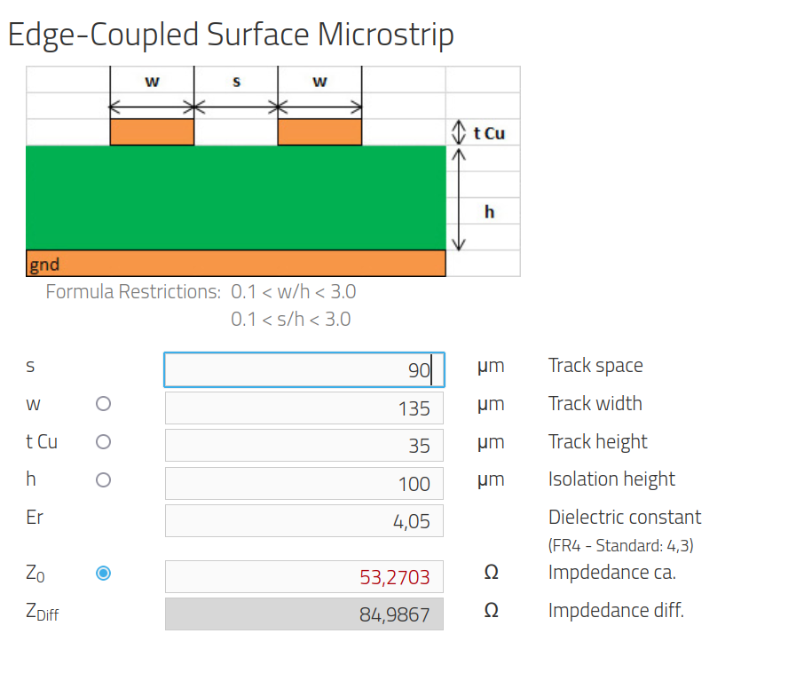
You don’t have to stick with the default stackup, though! After little deliberation, I switched to the “3313” stackup – with 4.05 Er and 0.1 mm thick prepreg between top and middle layers. It seems to be a tad more expensive, but it does look a bit easier to route in the small amount of space that I have. This led me to 0.135 mm / 0.09 mm pairs, while keeping the same 85 ohms differential impedance. Now, all I need to do is to enter these parameters into the “Net Classes” table, and whenever I press ‘6’, I’ll immediately start drawing a 85 ohm impedance differential pair.
Diffpair Drawing
The IC is placed, the diffpair parameters are tuned – we can start drawing. Remember, flipping the PCIe pair polarity isn’t a crime, it’s an obligation to make routing easier on yourself. Somehow, in this design it wasn’t needed even once.
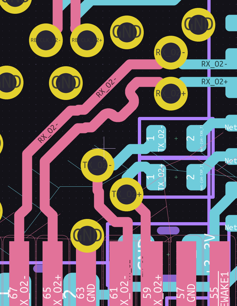
Remember, whenever your diffpair crosses from top to bottom layer or vice-versa, it also changes reference layers, from In1 to In2 respectively – and you’ll want to add ground vias near the diffpair vias, so that the ground return current can travel along the pair, too. As usual, four vias are ideal, three are good, two are okay, and one is non-ideal but better than zero.
Once we’ve drawn diffpairs and added ground vias, there’s one last thing to take care of. While PCIe pairs don’t have to all be the same length, the two traces that each pair consists of, do have to be the same end to end. For that, you can use the differential pair skew correction tool – mapped to 9 on the keyboard. It will add a wiggle to the longer track, in the spot where a wiggle would fit best.
All The Layers
When drawing boards, you can often use one GND and one VCC internal layer – as technically, both VCC and GND can be used as reference planes for high-speed signals. However, since we’re crossing diffpairs between top and bottom layers, they would then have different references, and this is still unexplored territory for me – I’m not sure whether there’d be return current problems. I’ve started out with one 1.2 V and one GND internal plane, but afterwards, as I was sanity-checking my boards and writing this article, I talked with other engineers, re-read an interesting comment thread under the first PCIe diffpair article, and decided to switch to having both internal planes as GND.
When it comes to the outer layers where diffpairs go, you’ll want to remove the ground fill or move it away, so that the ground fill around the pair will affect the diffpair’s impedance – you are highly likely see a ground keepout if you take a look at any PCIe card you own. Here, I am going to route diffpairs on the outer layers, but I’m not not going to completely remove ground on these, using keepouts instead. First off, having ground is cool – it’s extra copper that can help dissipate heat from the switch, or the switching regulator, or both. Second thing is – JLCPCB has been weird about ground fills on dense boards recently, and I’ll want to avoid that.
How far should the keepout go, then? The 5L rule (five trace widths away) is a good one, or you can just keepout the entire area where you’re pulling the differential pairs. For us, 5L means 5 * 0.135 mm, or 0.685 mm distance between the pair/via and the ground fill. The 5L rule isn’t a hard limit – keep to it as much as possible, but don’t stress about having a few vias here and there. Remember, when wiring up PCIe, it’s important that the string is wet.
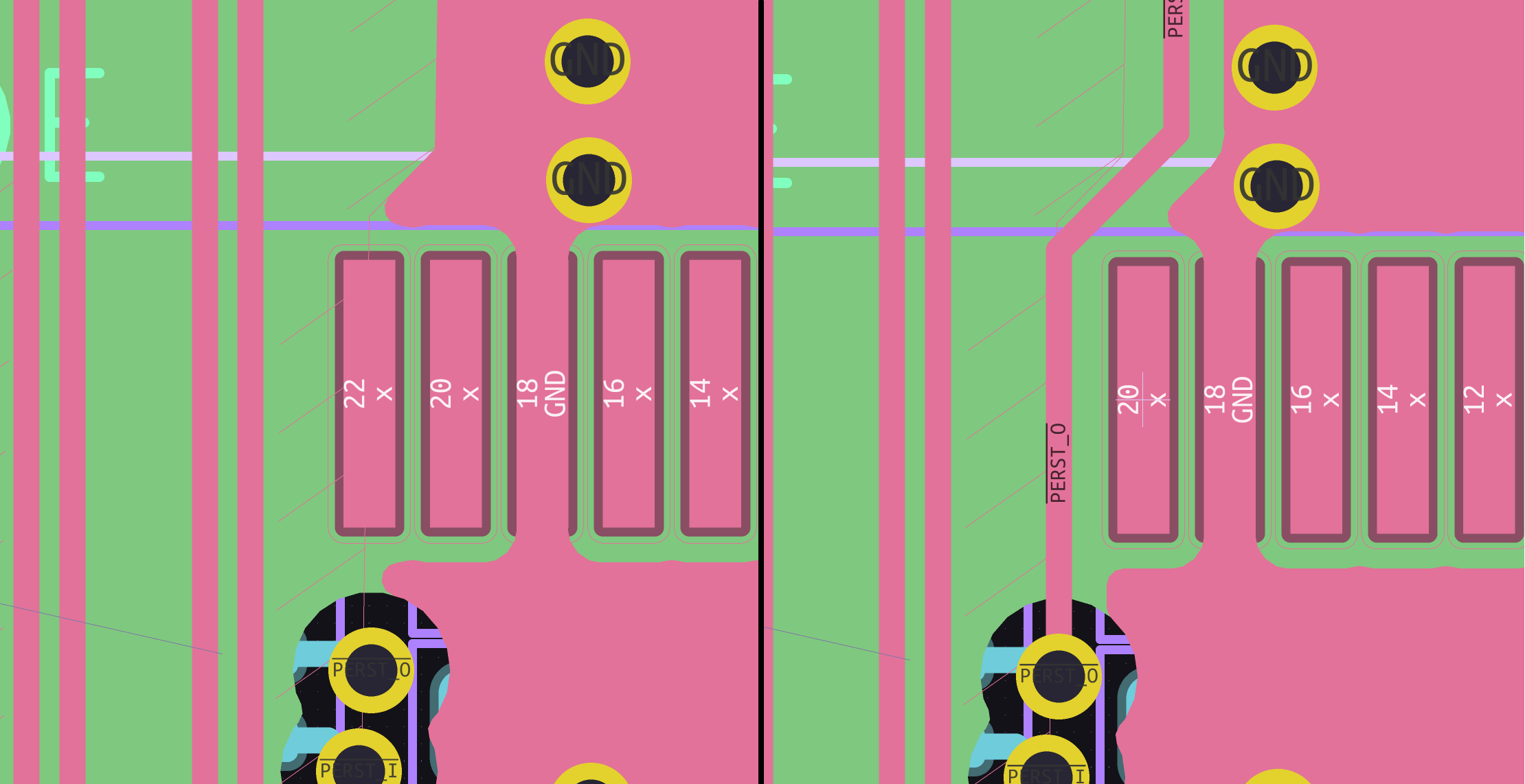
After we wire up PCIe and power signals, there are a few things left. It might be tempting to route them on the inner ground layers – do your best to fight the temptation, however, as there’s usually a better way; having unbroken inner planes is widely accepted to be good mojo for diffpairs, and for signals in general. Instead, consider other nonstandard options that are less of a sin – for instance, it’s okay to remove solder pads from a footprint if the pad is unused, and that’s what I’m going to do to pull one of the PERST signals through the top layer.
Mistakes And Problems
A PCIe switch functions at high speeds, so it makes sense that power consumption could be a bit harsh, and same would go for heat dissipation – indeed, you will see higher-port-count chips like these covered with glued-on heatsinks on Chinese adapters; My main concern is power consumption – a M.2 E-key card is expected to consume 2 A at most, and the peak power consumption of the switch, together with the inserted card itself, might exceed this budget for sure.
Every board can be a small experiment, and this one’s definitely got a few things I’ve never tried before. I’ve added this board to my last PCB order, and once it arrives, I’ll share the end result with you all, one way or another. Until then, the files are on GitHub, and I hope that this board’s story gives you plenty of insights into designing with PCIe!