
![pcb-design-review:-tinysparrow,-a-module-for-can-hacking-needs-[hackaday]](https://i0.wp.com/upmytech.com/wp-content/uploads/2024/04/176794-pcb-design-review-tinysparrow-a-module-for-can-hacking-needs-hackaday-scaled.jpg?resize=800%2C445&ssl=1)
PCB Design Review: Tinysparrow, A Module For CAN Hacking Needs [Hackaday]

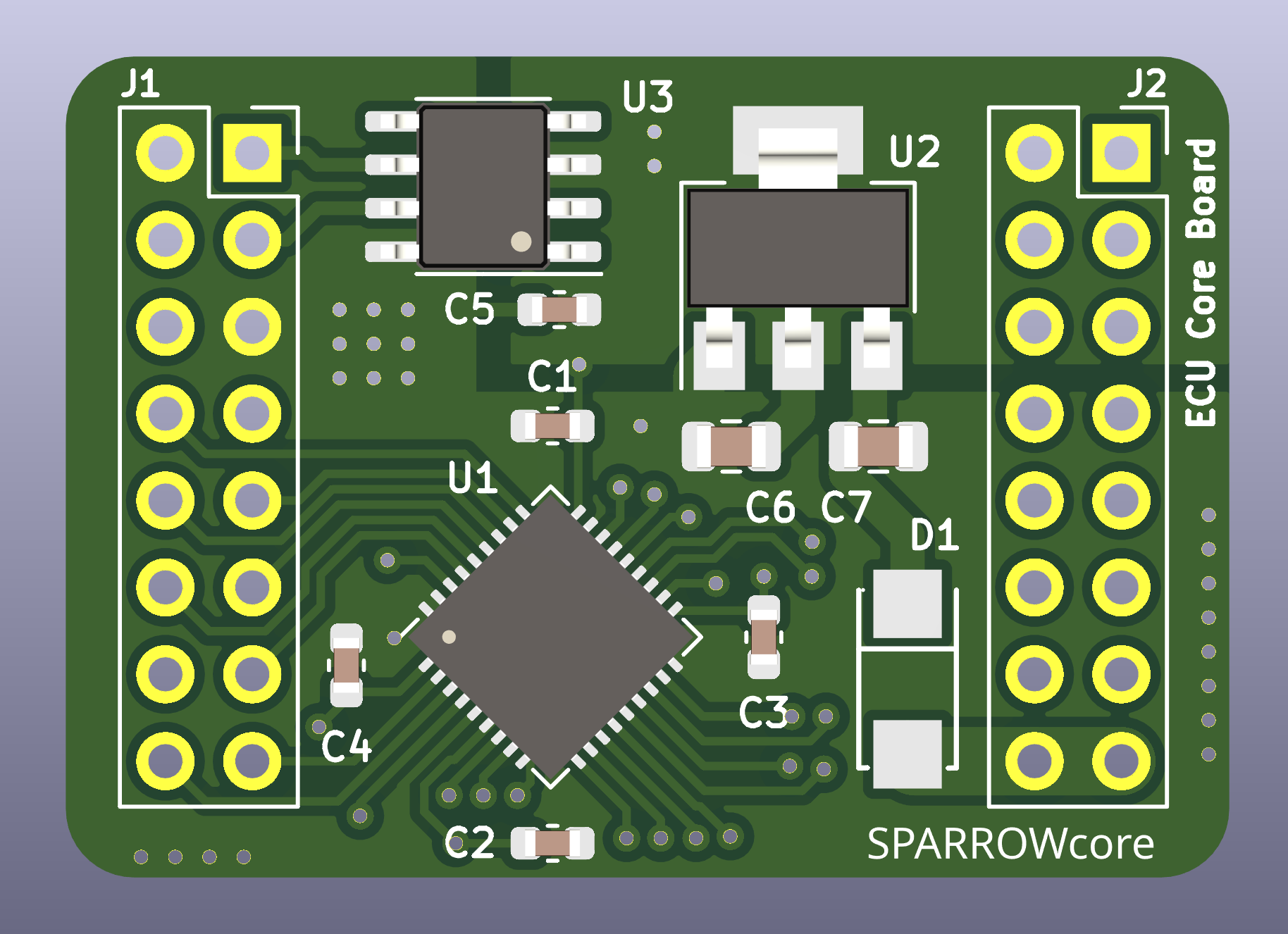
I enjoy seeing modules that can make designing other devices easier, and when I did a call for design reviews, [enp6s0] has submitted one such board to us. It’s a module called TinySparrow (GitHub), that helps you build your own vehicle ECUs and any other CAN-enabled things. With a microcontroller, plenty of GPIOs, a linear regulator and a CAN transceiver already onboard, this board has more than enough kick for anyone in hobbyist-range automotive space – and it’s surprisingly tiny!
You could build a lot of things around this module – a CAN bus analyzer or sniffer, a custom peripheral for car dashes, or even a full-blown ECU. You can even design any hardware for a robot or a piece of industrial technology that uses CAN for its backbone – we’ve all seen a few of those! It’s a great board, but it uses six layers. We’ll see if we can do something about that here.
Modules like TinySparrow will make your PCBs cheaper while ordering, too! Thanks to the carefully routed microcontroller and the CAN transmitter, whatever board you design around this chip definitely wouldn’t need six layers like this one does – and, unlike designing your own board, you can use someone’s well-tested and tailored libraries and reference circuits!
With TinySparrow, you save a lot of time, effort and money whenever you want to design a car or industrial accessory. After looking at the board files, my proposal for helping today’s board is – like last time – to make its production cheaper, so that more people can get this board into their hands if the creator ever does try and manufacture it. I also have some tips to make future improvements on this design easier, and make it more friendly for its userbase.
More Layers Not Always Better
Every single pin of the microcontroller is broken out – this matters a lot for such a module. It’s seriouslty annoying when you try to squeeze the most out of the onboard MCU, only to find out that the GPIOs broken out don’t expose one of the critical pins you need. I value such module designs a ton and I think people should be aware of their existence, which is why I’ve just spent time highlighting its strengths.
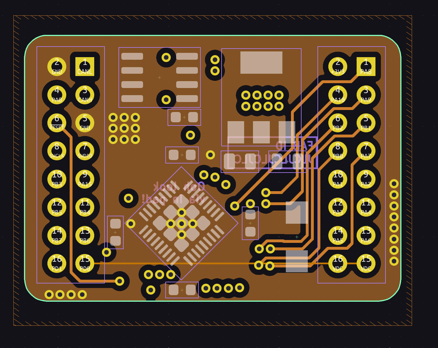


So about those layers. On one hand, this is justifiable for how tiny this design is. Three of these layers contain traces, two are uninterrupted ground fills, and another layer is 3.3 V. This is wonderful for signal integrity, and perhaps this board could really use an extra SI kick. Still, today, I would like to show you how to free up two of the layers, however – in part in case the author struggled to fit things on 4 layers, and in part to show how it’s done.
Six-layer layouts give you superiour signal integrity and a lot of space to route your traces. Often, six-layer boards are nigh unavoidable, like when doing high-speed USB-C altmodes with certain kinds of connectors. However, if these same features could be smooshed down onto four layers, it would be significantly cheaper both for the PCB and assembly.
So let’s get rid of two layers. As you can see, the layers are kinda full, so, some traces would need to be moved. For that, let’s look into the trace layout on this board. The board looks like it exceeds four-layer routing space provisions by a fair bit, but I can show you how it’s not the case!
Tweak The Defaults
For a start, let’s talk about default parameters, something that ends up limiting this board’s design. This board uses all default KiCad parameters – track widths, clearances, via diameters, and zone values. They are conservative, which is helpful for i.e. etching your own boards, but you lose that benefit if you just order the board, something inevitable at six layers. Let’s go through the distances on this board and see which values we can use while still being totally safe for manufacturing. After we dial the values down, we will have a lot more freedom for rerouting this board!
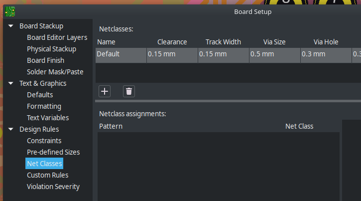
Track width is at 0.25 mm by default, but it can go as low as 6 mil on any self-respecting fab. Same for the 0.2 mm clearances – they can go to 6 mil too. On 4-layer and 6-layer boards, you can go down to 0.09 mm / 0.09 mm, which especially helps with diffpair layout, but also helps you pull track bundles from point to point.
Vias are 0.8 mm / 0.4 mm (ring width/drill width), which is huge – you can safely drop down to 0.6 mm / 0.4mm on 2-layer boards. At JLCPCB and other fabs, you can drop down to 0.5 mm / 0.3 mm on 4-layer and beyond without paying extra, but even smaller drill sizes tend to cost quite a bit more, so I don’t recommend you use them. As for zone clearances, the default 0.5 mm / 0.25 mm (clearance/minimum width) zone settings are okay, but decreasing them to something like 0.2 mm/ 0.2 mm or lower will help your fills get into tighter spots. On the other hand, solderability of the module’s pin headers will be somewhat worse with solid fills on GND – I would recommend that you use thermals for such boards.
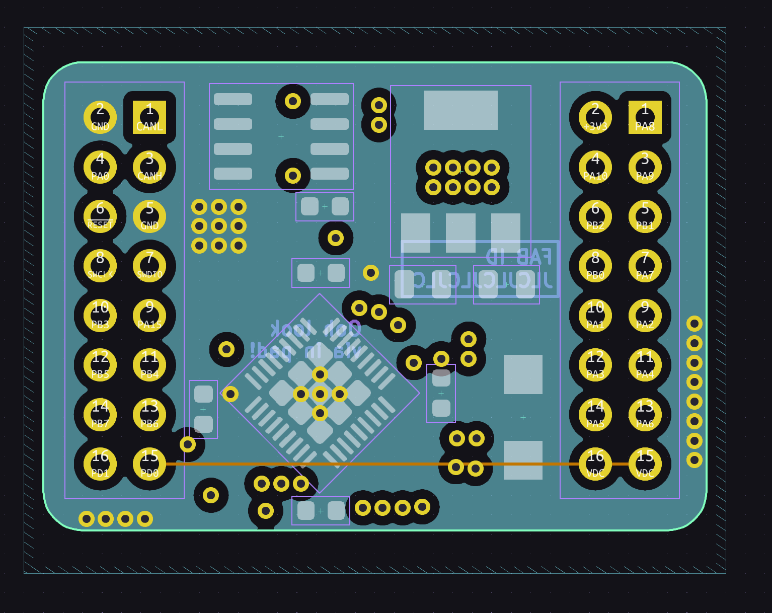
Let’s bulk edit these values! Switching track width to 0.15 mm and via size to 0.5 mm / 0.3 mm, suddenly, a lot of space has cleared up. I was thinking about rotating the microcontroller to allow for higher track density, but now I’m not even sure this is really called for.
Module Pinout
When you design a module like this and expect to have it be used on your and especially others’ boards, changing the pinout is to be done with care – I would know. However, I have strong arguments for why this module deserves a breaking change like that.
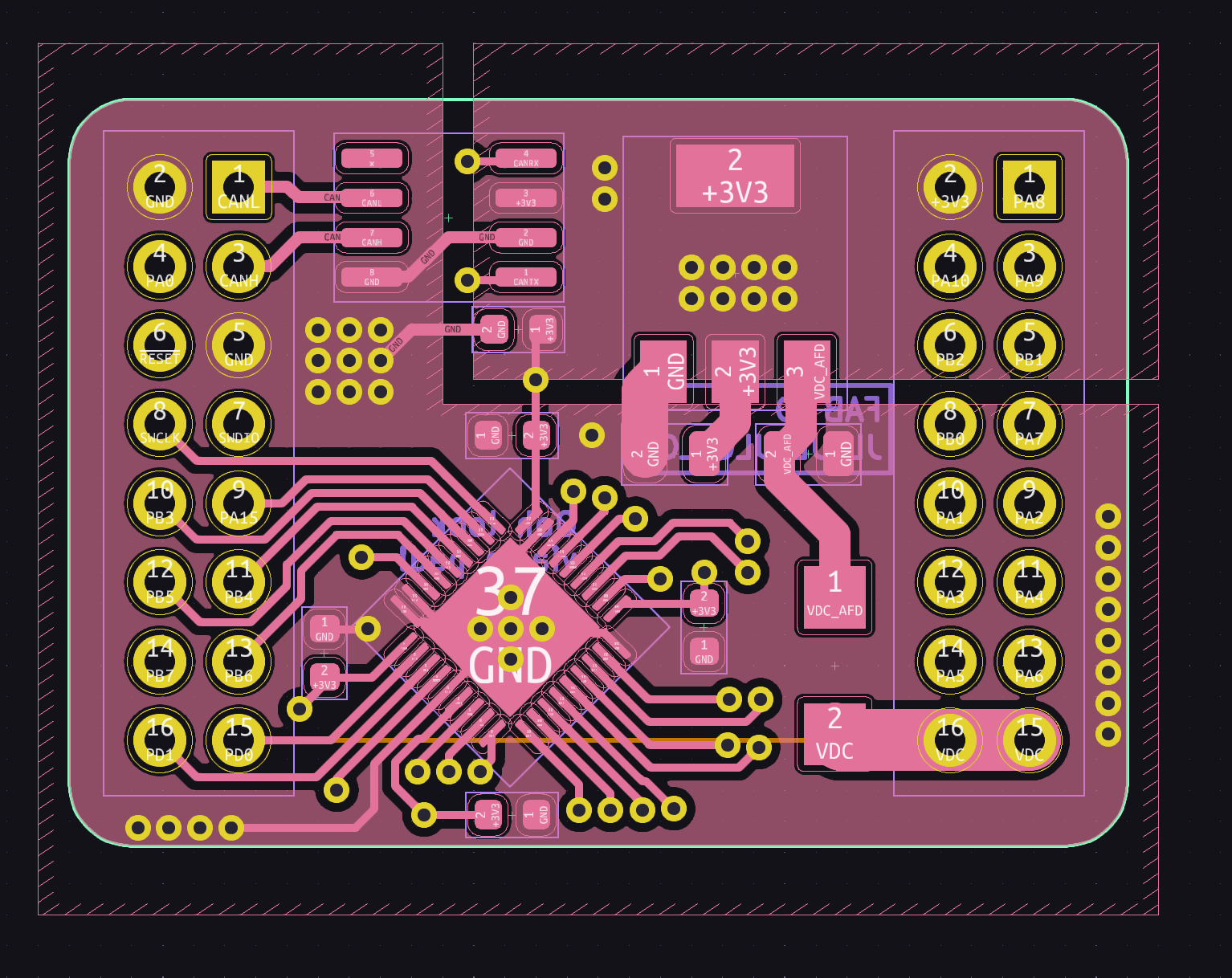
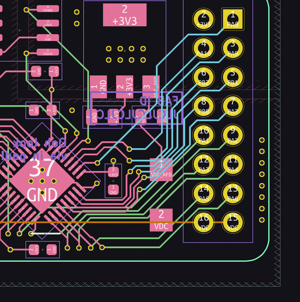
For a start, the module’s GND pins are far and few between – there are only two of them at the CAN header, whereas the module’s actual power inputs and outputs (VDC and 3.3 V) are on the opposide side. This will at least somewhat compromise the return currents for both power and CAN. Remember, there’s a reason we no longer put GND on the opposite side of VCC on modern chips, the way we used to do on DIP-package-era logic ICs.
So, the pin assortment ought to be tweaked. For instance, VDC doesn’t require two pins on the pin header – one of them would be enough, given that the module’s current consumption is quite low. I do acknowledge that breaking pinout changes are quite harmful, but you also have to make sure you make them before the module’s popularity increases. Learning from the Arduino example, the earlier you can make such changes, the better, so if the author is free to replace one of the currently-VDC pins by GND, that will help. You could even add one more GND pin surrounding VFC, replacing one of the near-CAN GNDs with a GPIO – this makes it way, way harder to damage the MCU through accidental screwdriver/metal object/dust application.
Two Layers Removed In Two Minutes
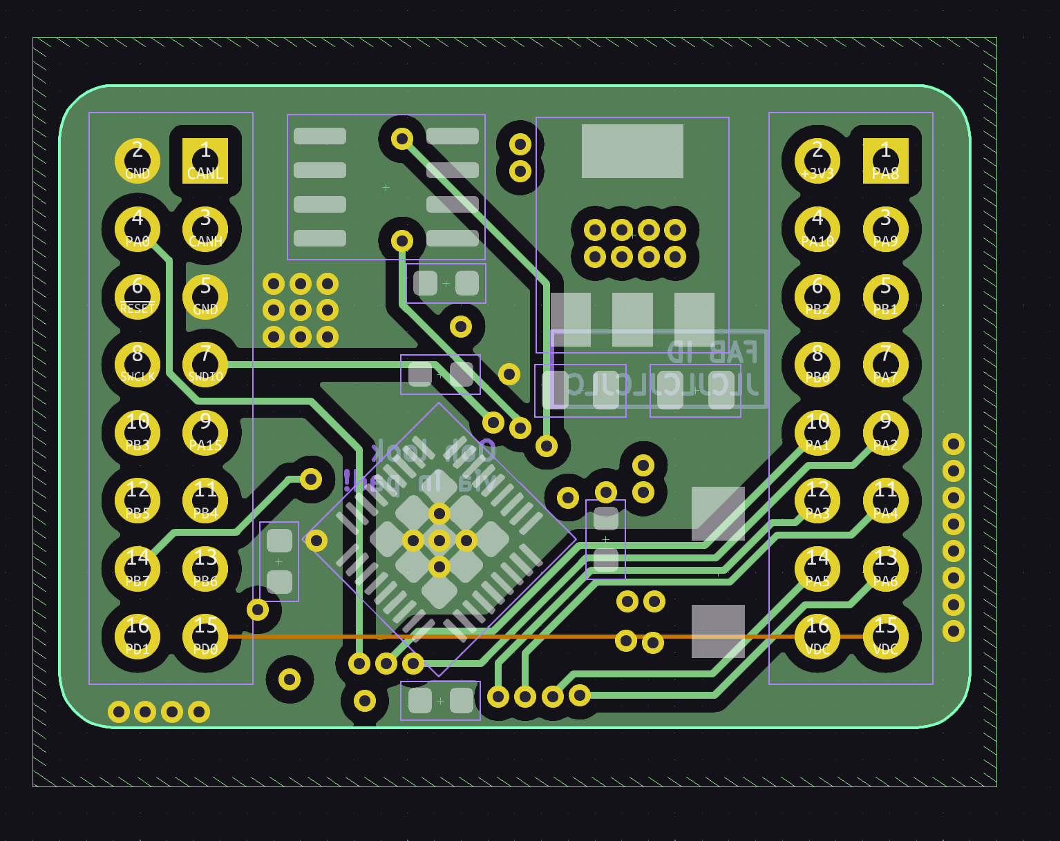
As for layer reduction, let’s look at where traces go. Disabling fill visibility, then selecting only F.Cu, In1.Cu, and In2.Cu, something becomes apparent. While the VIN and module routing on the top interferes with direct signal layout, you could easily move In1 and In2 signals to B.Cu (currently unoccupied).
So, how do you do this reroute? Actually, it took me about two or three minutes. First, move In1 tracks to B.Cu using Edit => Edit Track & Via Properties. Then, tweak the now B.Cu tracks to make sure they don’t overlay with In2.Cu tracks. Last step – move In2.Cu tracks to B.Cu using the same menu. Now we have two outer layers that carry tracks, and four layers that are completely empty, save for their fills – a classic arrangement.
Which layers to get rid of? Three of the now-internal layers have GND and one has 3.3 V. You can delete In3 and In4 by changing the board layer count to 4 in Board Setup menu, and decide what to do with the inner layers. There’s two options – SIG-GND-PWR-SIG, or SIG-GND-GND-SIG. For GND-PWR, the 3.3 V plane only wires up three microcontroller pins, but having it as a power plane improves power current distribution somewhat. Alternatively, you could get rid of the internal power plane, for a relatively classic GND-GND inner layer option, and put the 3.3 V pins on B.Cu – thanks to the F.Cu 3.3 V polygon that the board author added, most 3.3 V-connected elements on the board don’t make all that much use of the inner 3.3 V layer when it comes to power delivery.
By now, the work is already done, and it only took a short while. With four layers, the board is cheaper to manufacture, especially given that the author already took care to only put components on the top layer – props to them. There’s only a few things left that are of note for me.
Silkscreen, And Some Q&A
The silkscreen of this board could use a few additions, in my opinion. For a start, it doesn’t list the board version, which might just bite you, especially given the internal traces! This is true even more so if you’re making multiples of this board and selling it – it really helps your users to know which exact version of the module they have, so that they don’t have to read chip markings or deduce things by trace layout. My preferred format is %BOARDNAME% by %AUTHOR%, v%VERSION%, and this board could very much use a label like this, given that it’s a module.
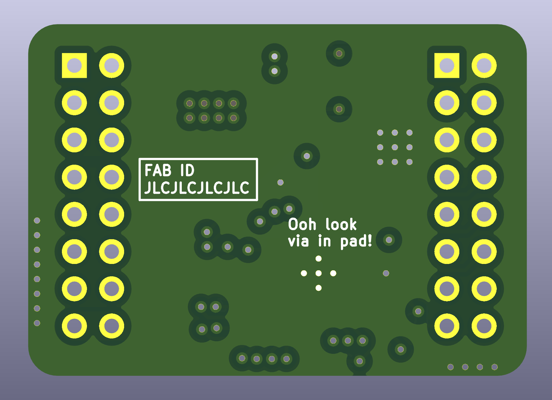
The back of the board is barren, save for the JLCJLCJLCJLC text that safeguards the board’s top layer and a small easter egg. That said, silkscreen is free! There are two options. First option: it could show the module pinout, for the users’ convenience. Second option: it could have some art, for the users’ emotional landscape in one way or another. Choose extra wisely, for both of these choices are wise to make.
Now, here’s a question for the readers – it’s about choosing which components to put onto such a module. This is a board used in an automotive environment – something that is not my domain of expertise, but I’ve read about it here and there, and I wonder if this module would require higher care. For instance, should you put protective elements for the CAN transceiver on this module? CAN termination? Some amount of GPIO protection? Or should these things be relegated to the carrier board, serving as impromptu documentation on the “here’s how you use it” question?
Remember – you, too, can submit your own PCB designs for my review! Send in your board into our tips line, with [design review] in the header, KiCad preferred, Git repository link desired but a ZIP file/Google Drive/DropBox link also works. Last but not least, let me know what you think about this feedback, of course – any notes of your own?