
PCB Design Review: HDMI To LVDS Sony Vaio LCD Devboard [Hackaday]
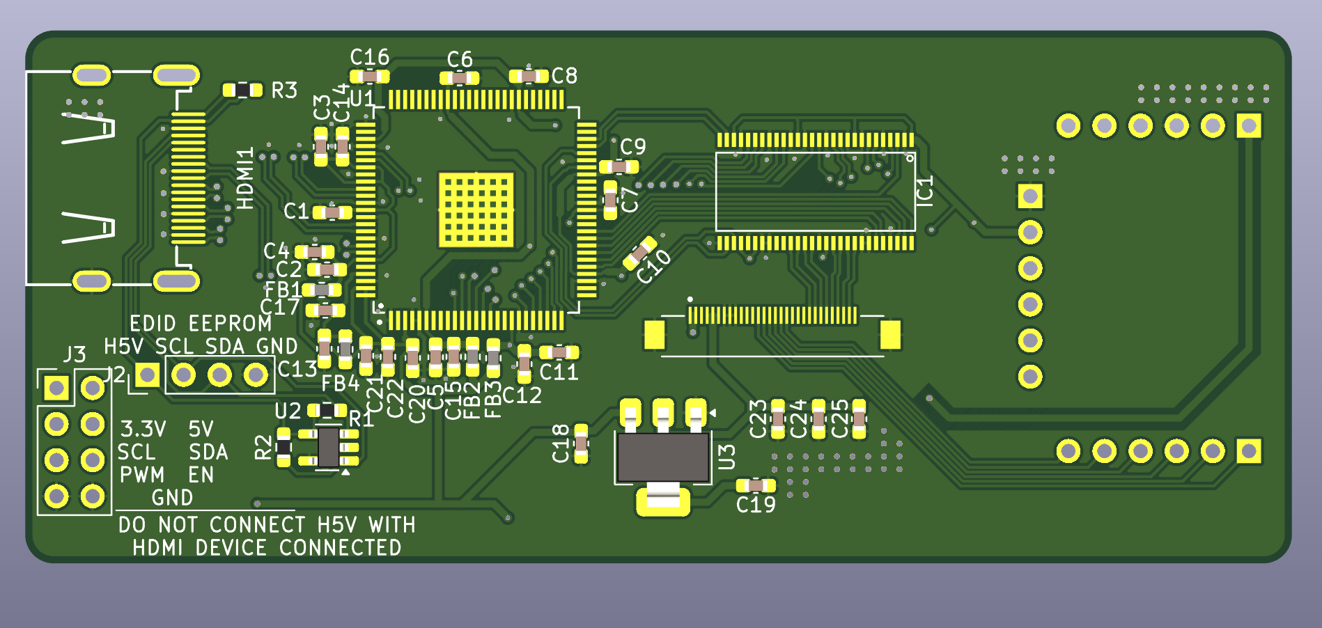
Today, we revisit another board from [Exentio] – a HDMI/DVI to LVDS transmitter for the Sony Vaio P display. This board is cool to review – it has a high-speed serial interface, a parallel interface, a healthy amount of power distribution that can be tricky to route, and many connectors to look over.
I’ve decided to show this review to you all because it demonstrates a PCB improvement concept we haven’t yet touched upon, that you should absolutely know about when doing board layout. Plus, I get a chance to talk about connector choice considerations!
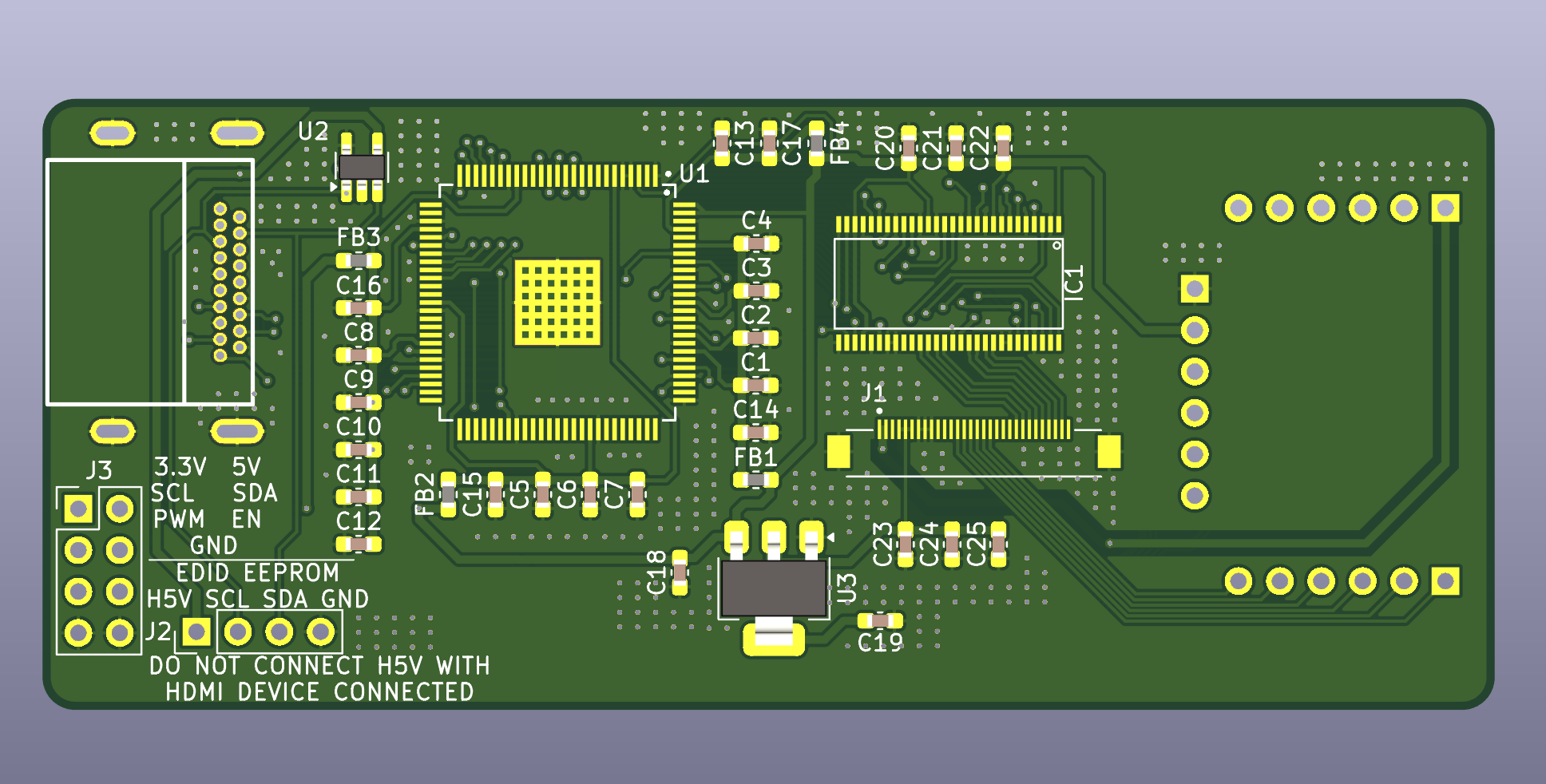
The board is lovely. It integrates the DPI-LVDS circuit we’ve previously reviewed, but also a HDMI to parallel RGB chip from Texas Instruments, TFP401, a chip appreciated enough that even Adafruit has adapters with it. The fun thing about this chip is that it doesn’t even handle EDID like the usual HDMI to RGB/LVDS chips you get on cheap Aliexpress boards. So, there’s no firmware to take care of – it just receives a HDMI/DVI signal, converts it into parallel RGB, then converts that to LVDS, and off to the display it goes. The downside is that you have to provide your own EDID with an EEPROM, but that isn’t that tricky.
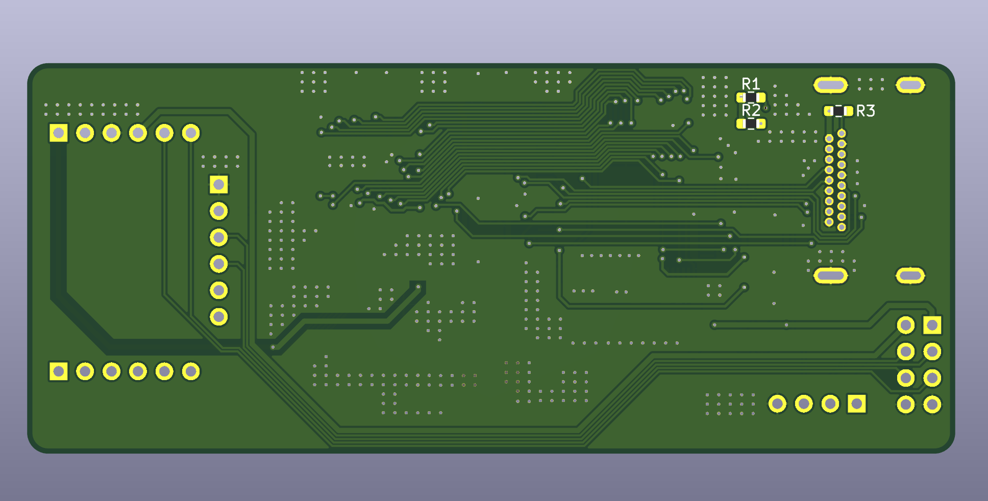
Again, this is a two-layer board, and, again, I like this – fitting tracks to the smallest possible space is a respectable and enjoyable challenge. This board has absolutely done well by this challenge. I do see how this board could be routed in an even better way, however, and it could be way way cleaner as a result. For a start, rotating the chip would improve the odds a whole lot.
The Chip Gets Rotated
When doing silicon layout, engineers generally try and make the resulting chip pinout as sensible as possible. There can be exceptions, of course. This rule means that there’s usually a single easy way to lay out a chip, and a few hard ways. You have to look at the pinout, try to notice the pin groups, and see how they align with your peripherals. Ignore this at your own peril.
The TFP401 chip has HDMI on one side and parallel RGB pins on the other. This board, however, currently has the chip rotated in a way that disadvantages the layout. This is an easy mistake to do initially – thankfully, even when the design is already finished, rotating the chip and rerouting it can pay off!
If you reroute this kind of board, not only you are more likely to get a functioning board, considering the high-speed signals, you’re also training yourself to distinguish good and subpar chip rotations as you’d be rerouting. In other words, it’s the kind of refactoring that makes you say “wow, that was way easier than the first time around”.
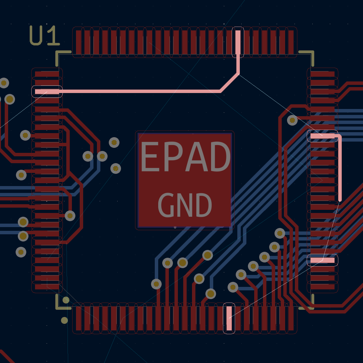
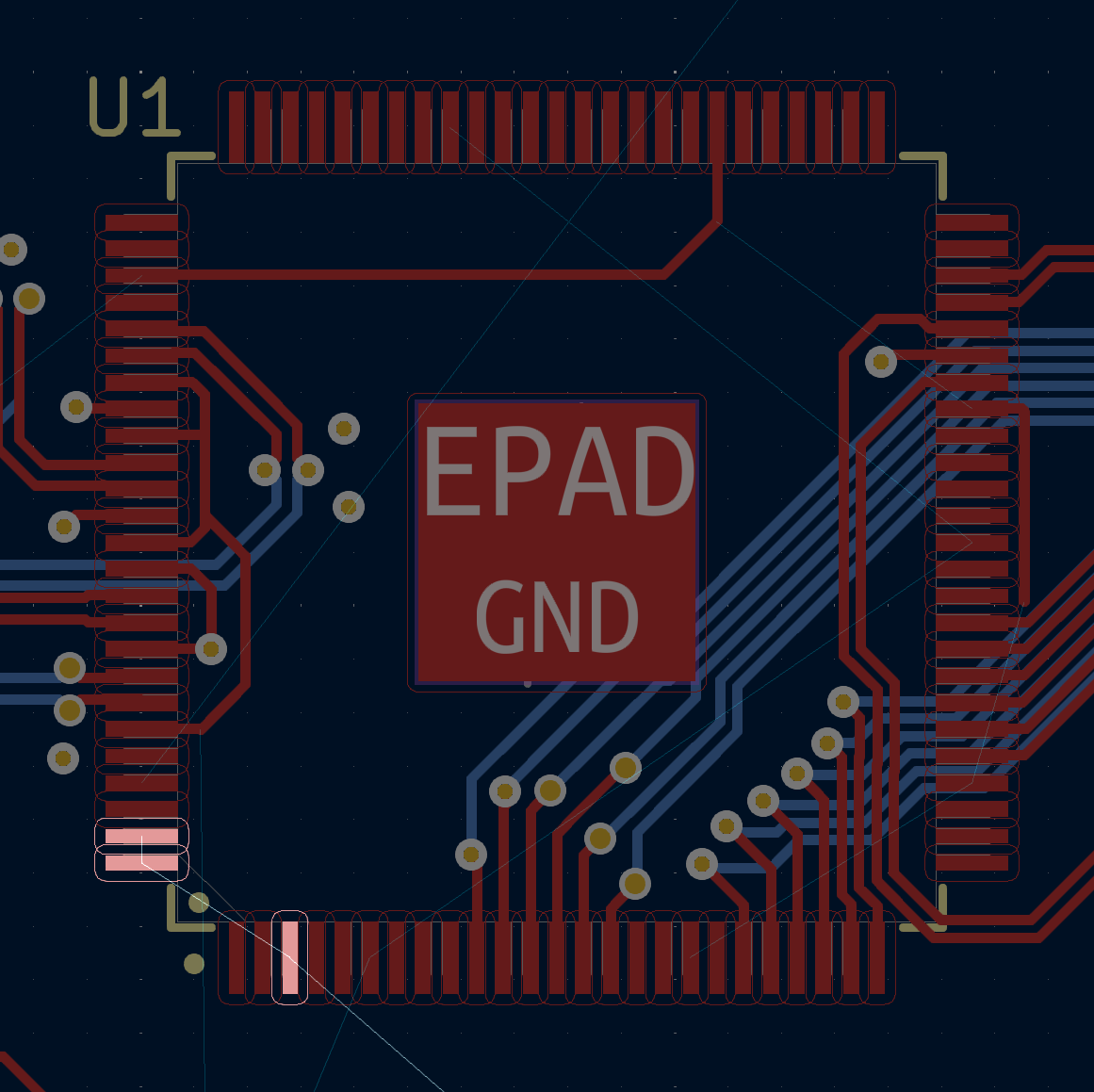
Lift, Clean Up, Rotate, Behold

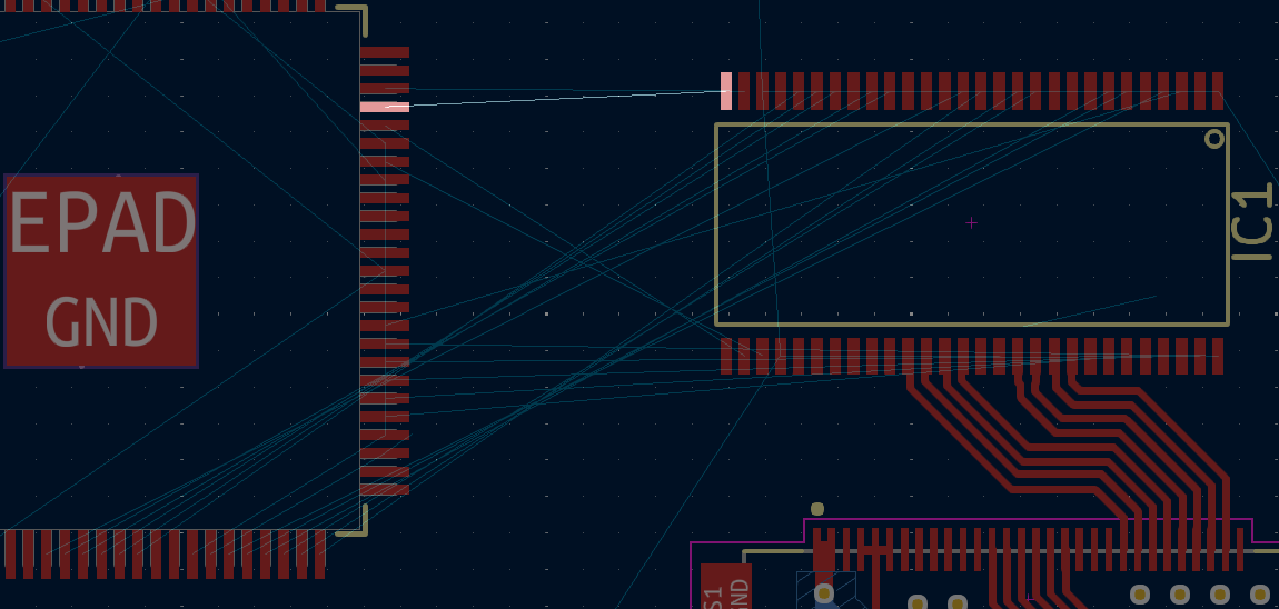
M and move it off the board. See the grey thin wires? They’re called ratsnest wires, and using them is the best way you can notice rotation issues. Seriously, the ratsnest wires are underrated in noticing such issues before they bite you. Let’s clean the chip’s surroundings up. First, see those capacitor groups? Move them away too, all the power pins are changing their locations anyway, we’ll reposition them later.
Box select the signal traces that previously went to the chip, and press Shift+Del to completely delete them from beginning to end – on this board, this is the quickest way to get to a quickly routable space. Every trace that went to the chip is now gone, and every unrelated trace stays. Make sure there’s a healthy amount of space between the chip and the HDMI port, but also between it and the DPI-LVDS converter – more or less the same center position is fine here.
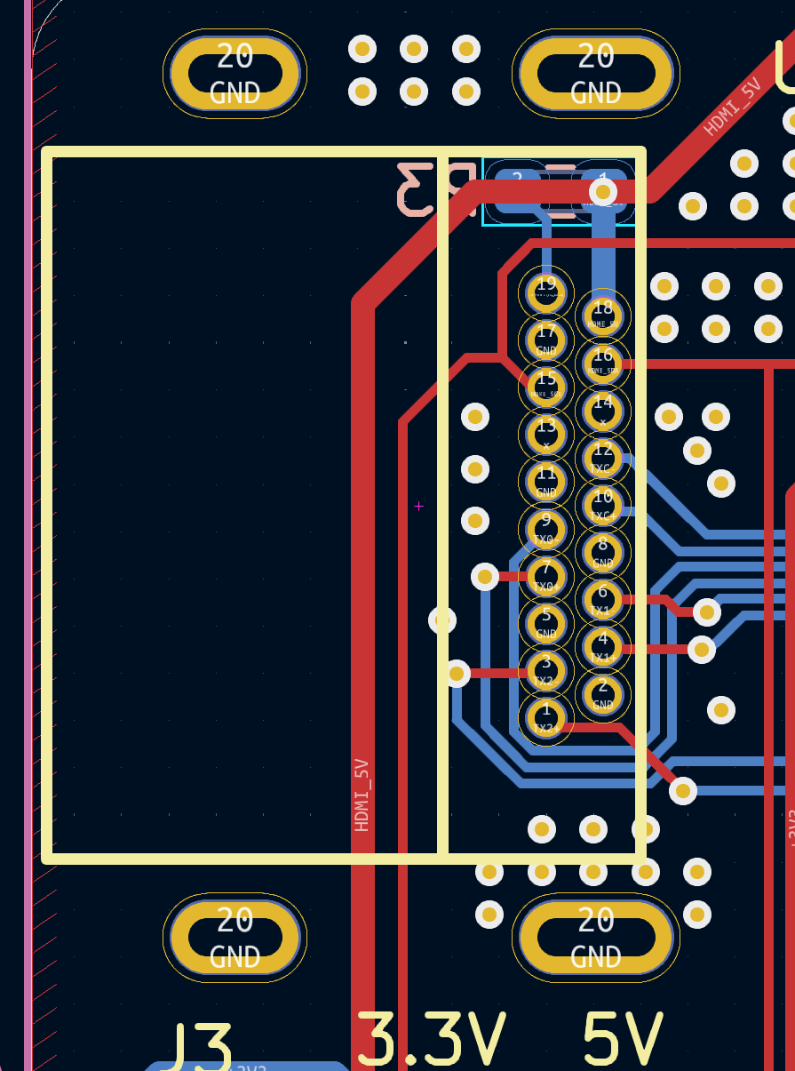
Speaking about HDMI, before routing, I will replace the THT signal pin HDMI connector with an SMT signal pin one. They’re way, way nicer to layout – the through-hole staggered pins mean that you have to run two of the diffpairs around the connector shell. Plus, they’re cheaper and easier to source too. [Exentio] picked this connector for expected sturdiness and solderability, and that is a valid choice, I’m just prioritizing ease of layout and easier sourcing.
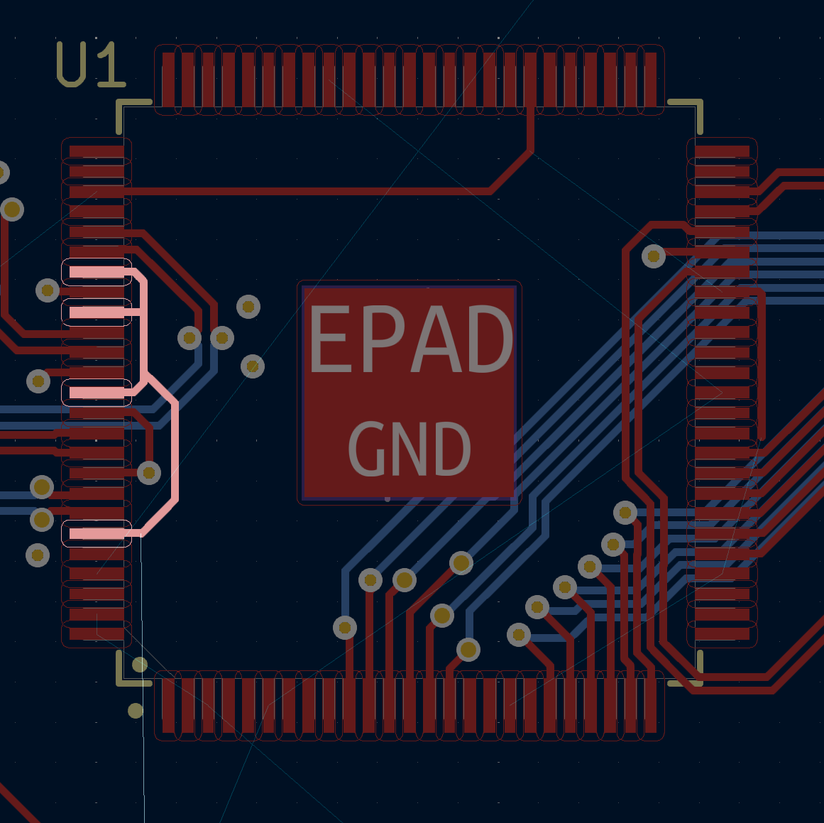
Reroute Time
With HDMI, not only is the order flipped, but the pair polarity is also flipped. Still, there are multiple things you could do here. You could flip the connector onto the opposite side of the board, or use a HDMI connector that’s flipped (harder to source but not impossible), or try to re-route the diffpairs as they are now. I’ll do the last one, since it’s the most fun one.
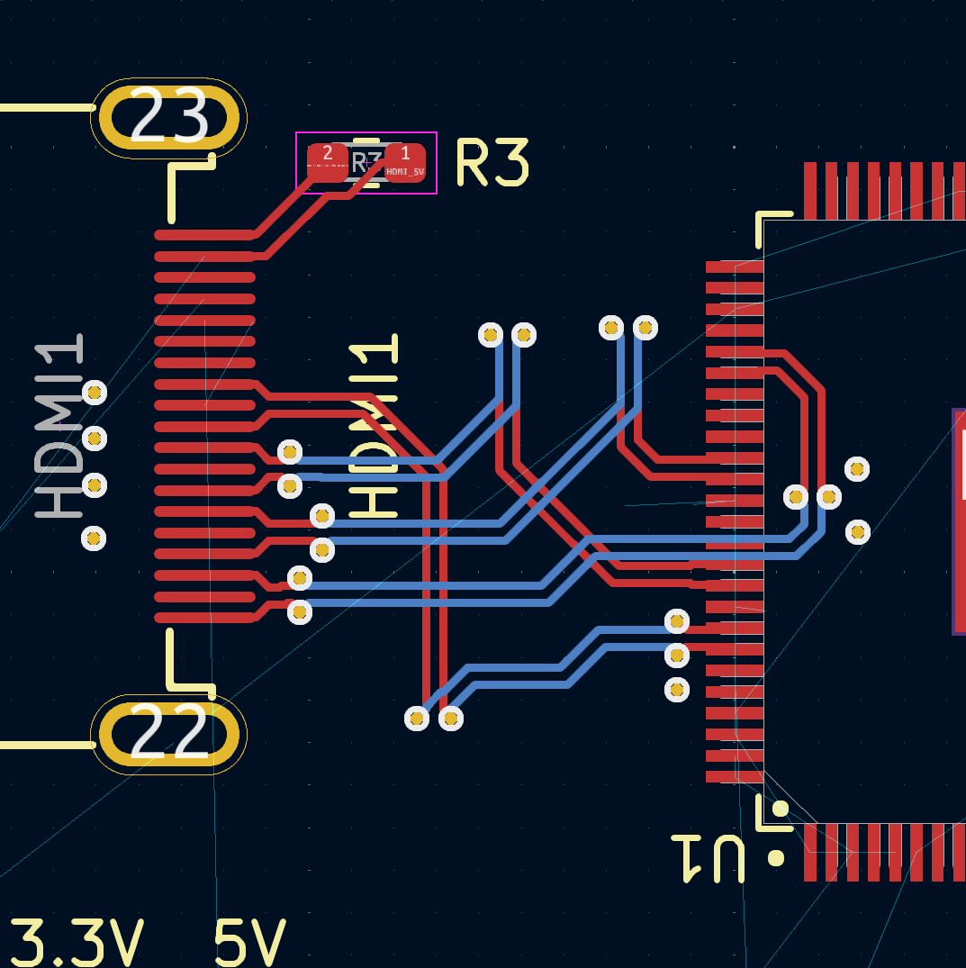
Now, what’s left is three bundles of parallel wires (R/G/B) and four individual tracks (EN/CLKIN/HSYNC/VSYNC) going to the DPI-LVDS chip. Since all four individual tracks are on the DPI-LVDS chip corners, I’ve decided that the parallel RGB pairs will go in the middle and the tracks will go around them. The biggest problem is flipping the bundles – you can do that under the HDMI chip or under the LVDS chip, I did it under the HDMI chip because it felt like there was just enough space there.
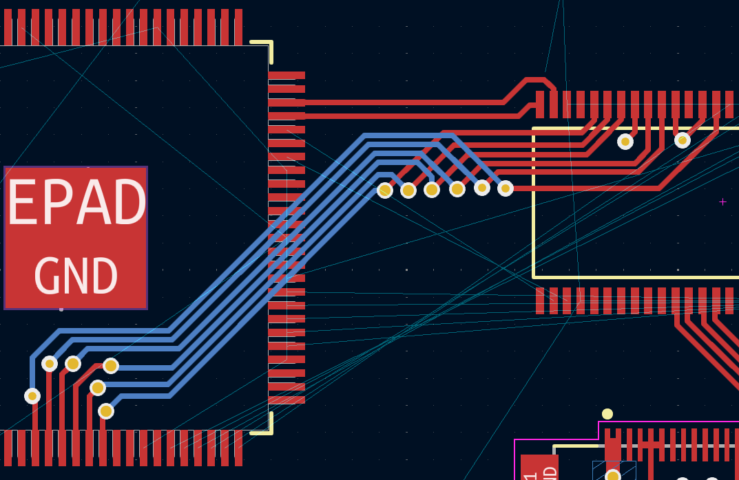

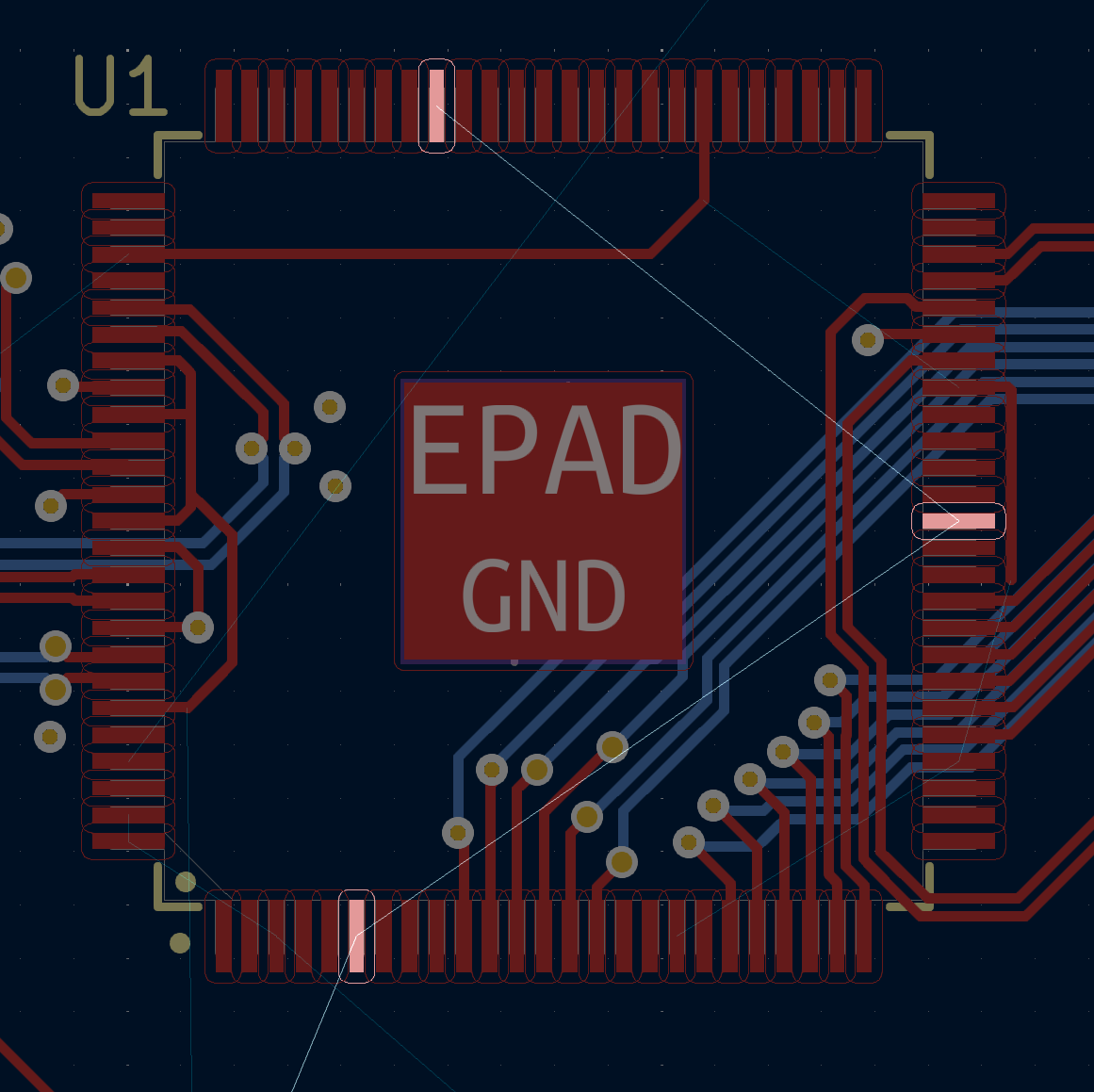
Here you can see how the three bundles progressed. They’re nice and tight, with some ground fills between the separate bundles and accompanying the wires. I’ve had to move the first bundle once to make room for flipping the last one, but other than that, things fit surprisingly nicely. The bundles don’t intersect each other’s paths, and that helps. If they did, I would probably consider rotating the DPI-LVDS chip together with the LVDS connector.

Power Pin Routing
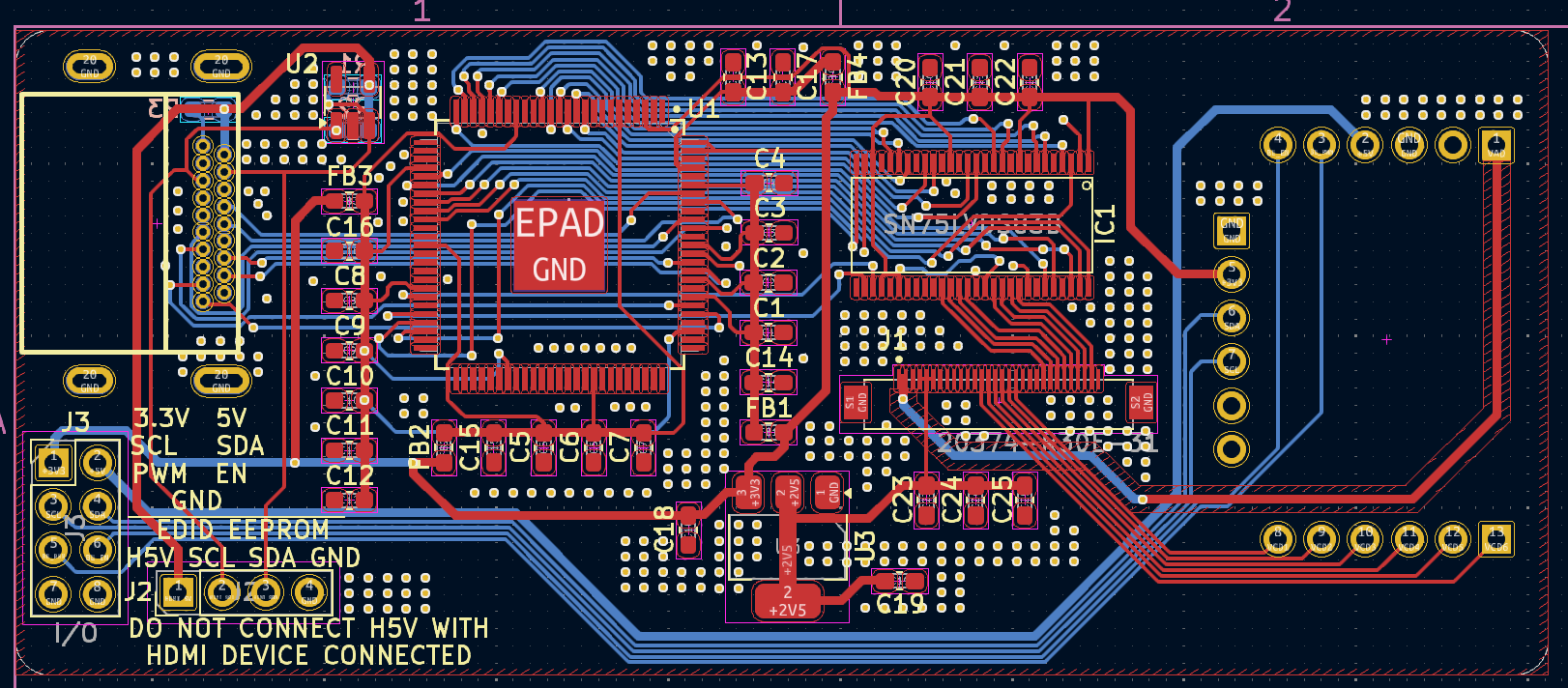
This is the thing you might get stuck on, at some point. The chip has whole four different groups of power pins – one direct 3.3 V input, and three separate 3.3 V inputs that you’re supposed to feed through Pi filters, for a cleaner power supply for all your analog needs. Use the “ (~)` key to highlight all four power nets of the chip – here’s how it will look.
I’d describe these as annoying, but they’re still routable. First, break apart the nice cap groups for the four rails – they’re nice visually, but they’re not great for power delivery. Remember – one capacitor per IC power pin is the platonic ideal, and each of these capacitors has to actually be placed close to a power pin, with a short path to ground too.
I started with the 3.3V feed, and then placed a couple of ferrites to nearby power rails. Then, I went through each of the power rails, starting with the simplest, pulling power tracks where it seemed viable. In the end, I could place all the ferrites near the actual 3.3V supply point. A 3.3V power plane could be fun on this board, and would probably be very much called for if we wanted to do FCC testing for this board, but for now, it’s not required.

Long story short, here’s the “rest of the owl” pictures. Remember – for power tracks, wherever you can make them thicker, make them thicker. They will drop all that less voltage, and they will look like dedicated power tracks, too. Also, don’t forget about GND! Highlight the GND net, then make sure that each GND point has a via directly near it, going to the bottom layer ground plane, with ground now even more abundant than before.

After this layout was done, there were only cosmetic fixes left. Things like trace keepout that I’m still maintaining, feeding 3.3 V everywhere it was called for. I suppose I would add a 5 V to 3.3 V linear regulator footprint onto this board, just because it would make bringup much easier, but it’s such a small change that it could even be bodged onto this PCB later with little hassle. This board is, all things considered, wonderfully hackable already.
Closing Statement
Here’s the end result of the board re-layout. It’s even cleaner than before, with improvements to both high-speed tracks and power distribution, and I hope it’s been a fun example about rotating your chips properly, something you could reasonably overlook on a board of yours.
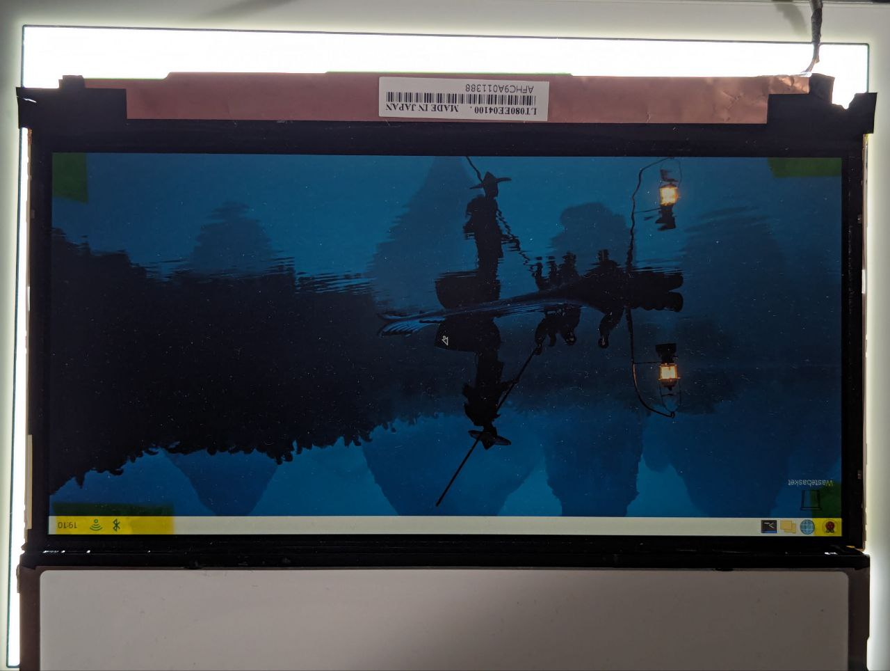
As an outro to this review, here’s some good news. That DPI-LVDS board we’ve reviewed last time? It works! Which means that the DPI and LVDS parts of this HDMI-LVDS board should also work. Nothing is fundamentally broken to the best of our perception, [Exentio] has designed a working RPi config, and, as such, one of the more challenging parts of the Sony Vaio rebuild design is now complete – we only need to tinker with the backlight now.
As usual, if you would like a design review for your board, submit a tip to us with [design review] in the title, linking to your board files. KiCad design files strongly preferred, both repository-stored files (GitHub/GitLab/etc) and shady Google Drive/Dropbox/etc .zip links are accepted.