
PCB Design Review: HAB Tracker With ATMega328P [Hackaday]

Welcome to the Design Review Central! [VE3SVF] sends us their board, and it’s a HAB (High Altitude Balloon) tracker board. It’s got the venerable ATMega28P on it, a LoRa modem and a GPS module, and it can be powered from a LiIon battery. Stick this board with its battery onto a high-altitude balloon, have it wake up and transmit your coordinates every once in a while, and eventually you’ll find it in a field – if you’re lucky. Oherwise, it will get stuck hanging on a tree branch, and you will have to use a quadcopter to try and get it down, and then, in all likelihood, a second quadcopter so that you can free the first one. Or go get a long ladder.
The ATMega328P is tried and true, and while it’s been rising in price, it’s still available – with even an updated version that sports a few more peripherals; most importantly, you’re sure to find a 328P in your drawer, if not multiple. Apart from that, the board uses two modules from a Chinese manufacturer, G-Nice, for both GPS and Lora. Both of these modules are cheap, making this tracker all that more accessible; I could easily see this project being sold as a “build your own beacon” kit!
Let’s make it maybe a little nicer, maybe a little cheaper, and maybe decrease the power consumption a tad along the way. We’ll use some of the old tricks, a few new ones, and talk about project-specific aspects that might be easy to miss.
The Low Hanging Fruit
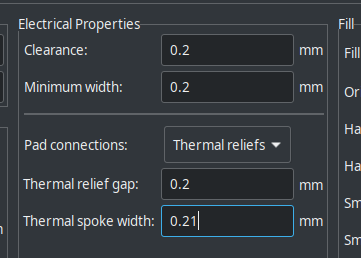
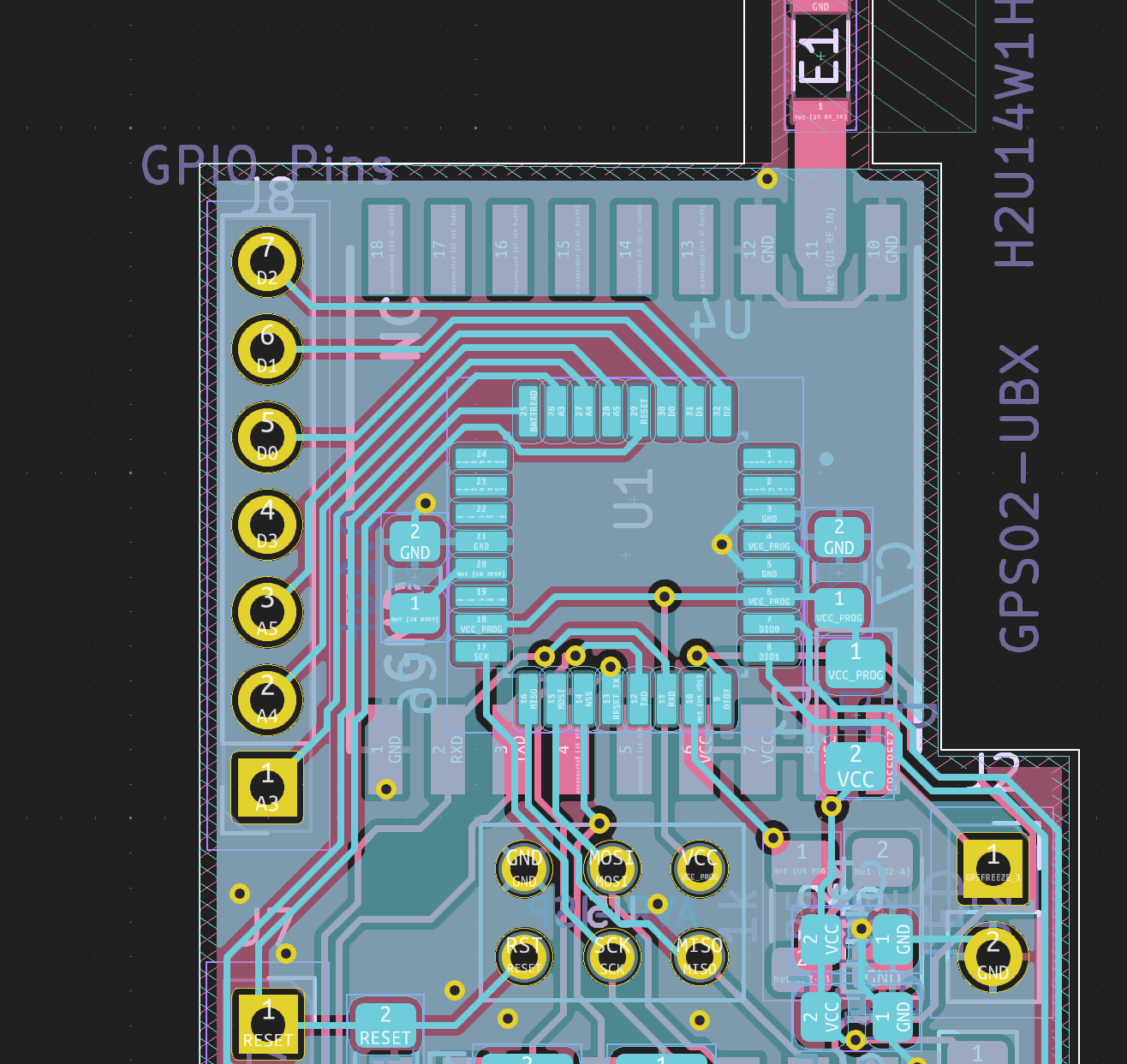
This board has four layers, which is nice because you get more ground and more routing space for a tiny price increase these days. This board doesn’t add fills on inner layers, but that is an easy fix – just select one of the GND power planes and tick the In1/In2.Cu boxes in their settings. Another thing to tweak in zone settings is zone clearance and minimum thickness – default KiCad clearances are way too conservative, setting them to something like 0.2 mm / 0.2 mm is a good idea. That improves ground connectivity, and also lets us get rid of ground tracks that would otherwise be necessary to bring ground to different connectors.
The inner layers have ground, and ground on all layers can reach further, too. That said, the inner layers benefit from being completely free – that’s when you get the best return current flow. Remember, each track, whether signal or power, needs its ground return path, and if you don’t provide a direct clean one, electricity will find a way. That, in turn, results in noise, both received and emitted, as well as possible instabilities.
In particular, the ISP flashing header had a lot of low-hanging fruit; tracks that were pulled on inner layers but could as well go on top/bottom layers. Many tracks could be snaked between GPS and LoRa module pads, too – the gaps are wide enough, that even a 0.2 mm track feels comfortable in there, and you could probably pull two if you dropped down to 0.15 mm, which is still safe with most fabs.
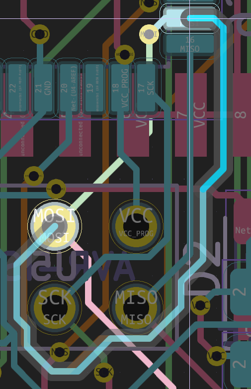
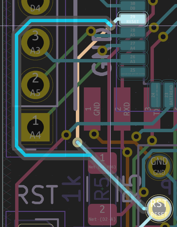
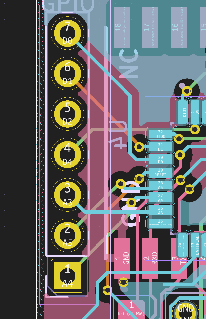
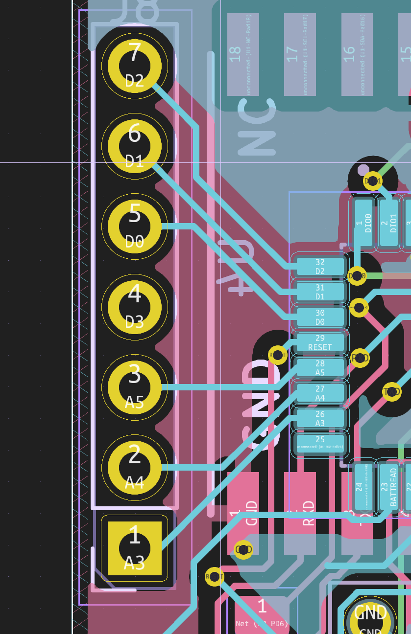
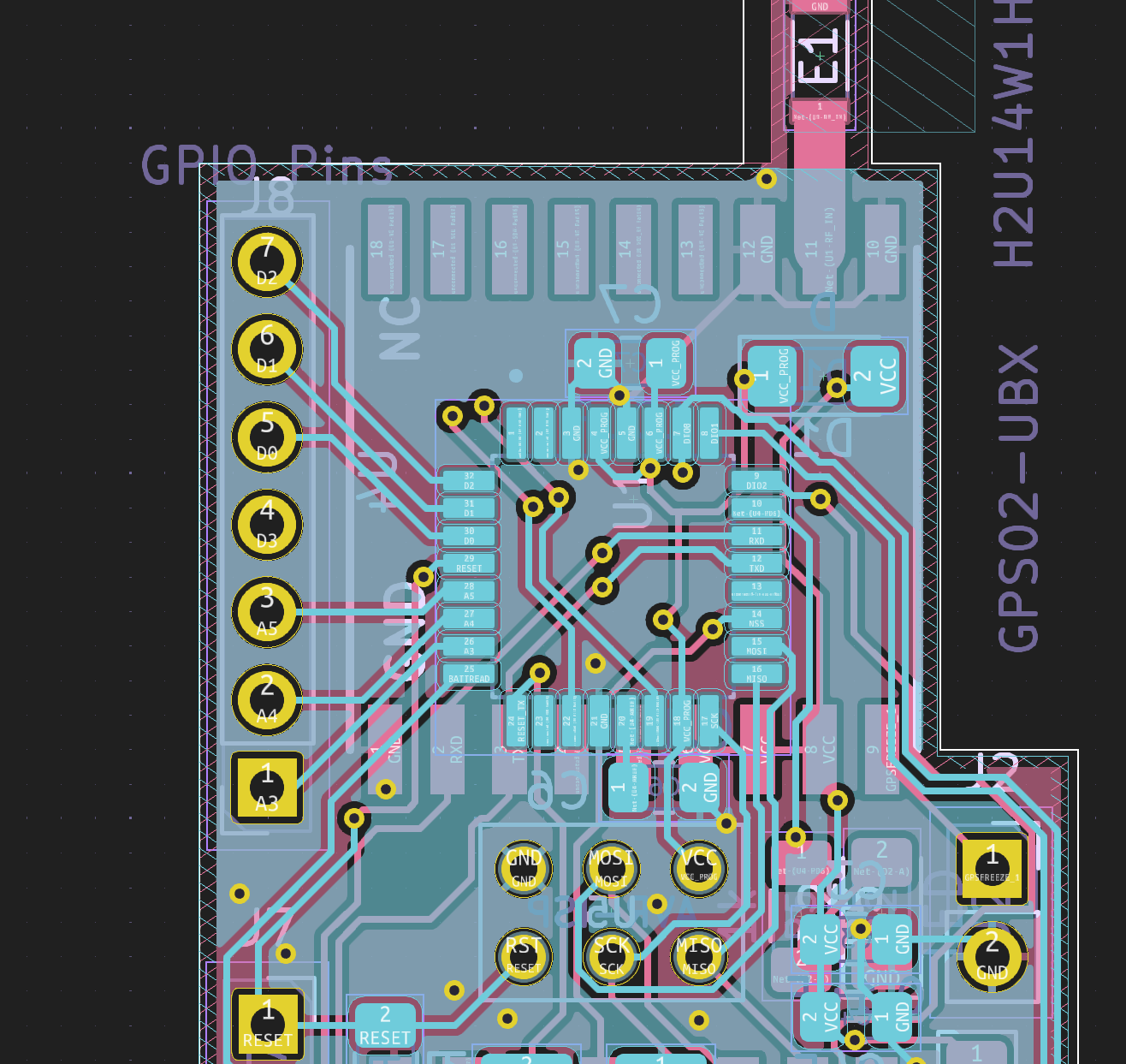
And, after a dozen minutes of work, the inner layers are free. A surprising amount of space could be found – for instance, the three DIO tracks nicely went along the right edge of the board. More importantly, capacitors were moved closer to where they work best. In particular, the AREF capacitor is two vias and one long inner track apart, which won’t make for good analog decoupling. That did require moving the ATMega a bit upwards, but a judicious application of Del and Shift+Del on tracks, as well as some track dragging, made that move go quickly.
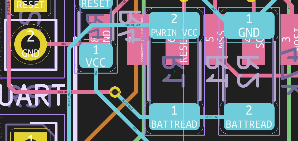
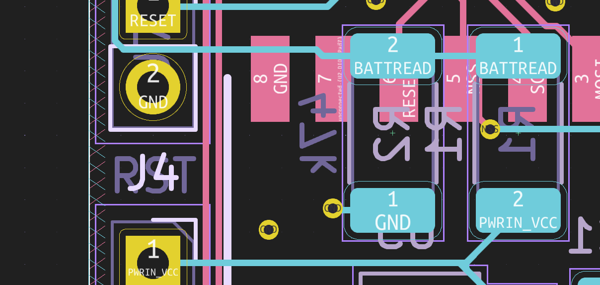
I could talk about component size choices, but they’re not meaningfully interfering with routing on the board – even the opposite, having one of the diodes be 1206 helps me avoid some vias. On the other hand, rotating the battery divider resistors and power regulators 180 degrees resulted in some good routing space freed up. And, looking at the board, the ATMega328P routing could perhaps use being rotated one turn clockwise, too. That’d make SPI routing cleaner, power tracks and analog pins shorter, and let us put capacitors at the sides, at the low low cost of having GPIO pins snake around a bit. However, here, the benefits aren’t necessarily as clear-cut as in previous articles; instead, it’s a time vs niceness tradeoff.
The Chip Gets Rotated, But Not Necessarily
Here, a conundrum. We could spend maybe a dozen more minutes and rotate the chip, or leave it be? Is the board going to be slightly nicer? Yes. Is this necessary? No. If you want to just order the board and go, it’s completely fair for you to press order and leave improvements of this grade for rev2. On the other hand, if the itch to improve your board is bad enough that the time investment doesn’t scare you out of it, give in and see yourself become better at PCB design. Worked for me.
There are hidden problems for such small redesigns, though. Remember, a redesign might have you reinstate a problem that you’ve successfully avoided with the original iteration, or, it can quickly become infeasible. I’ve had it happen, where a redesign that intended to add features and reduce complexity has become counter-productive midway through, so, I’ve had to stop myself from continuing and just order the board already. You’ll learn to keep track of these, but it does take keeping it in mind. Keep your Ctrl+Z’s ready, keep a copy of the files, or a Git commit, if you are doing something fundamental, and be ready to get a lesson in letting go.
I ended up rotating the chip, and the board did indeed become a bit nicer, but in ways that don’t solve any pressing problems. By the way, have you noticed something this board has done really well from the start? That’s component placement. The ways the LoRa module, GPS module, ATMega328P and the headers are positioned, I wouldn’t change anything about them. Maybe move the pin headers onto a 2.5 4mm grid so that you could expand this board with a perfboard if needed, but that one isn’t a must – this is a low weight board, after all, the headers are more for debugging than anything else.
Last Thoughts: Inner Layers And Antenna Choice
If you have internal layers, use them for ground or power fills, so that power and return currents can flow unrestricted. This is going to reduce both radiated and received emissions, as well as make power rails smoother, which feels mighty helpful considering this design has two radios on it and the GPS radio has a passive antenna.
Also, some fabs don’t want empty inner layers. Last year, JLCPCB started refusing boards with inner or outer layers more than 30% full, in what’s presumably an attempt to decrease the etching process costs, causing some people to redesign perfectly working PCBs with little notice. Combine this with a recent documentation overhaul that just so happened to turn some previously free options into paid ones, and if I were to guess, they are no longer able to keep running at a loss as much as they did, so, the age of golden offers at JLCPCB might soon to be over.
Our improvements ended up providing more than enough copper on top and bottom layers, that you could possibly switch this board to two-layer; again, cheaper ordering, possibly quicker manufacturing time, possibly cheaper PCBA. Isn’t a requirement, but it is nice when you can do it. If you are to keep the two extra layers, remember that on-board antennas need keepouts at least for a wide patch under them, if not for a good amount of space around them, and the keepout has to be on all layers. No tracks, no fills, no copper, do not pass go, do not collect 200.
Thicker tracks for power paths are good whenever you can afford them – and this board has plenty of space! I personally usually add them in last, and it’s not a problem here, but it’s most certainly a smarter decision to draw them thick first so that you don’t have to do a re-layout later.
It also does feel like you could consider an active antenna here. For a high-altitude balloon, sure, you’re way way more likely to get a fix and you’ve got a whole lot more time to do it, but I would guess improving your chances is worthwhile. Plus, I don’t know much about G-Nice’s modules, still yet to try out the one I purchased last year – it might be that this module is perfectly okay, but it concerns me these are meant to be footprint-compatible drop-in replacements for well-established company modules, with this specific module borrowing an U-Blox footprint, and as such, I don’t know how much to expect. An active antenna adds a fair of weight and size footprint, and it might be that everyone’s flying with passive antennas no worries, so I might be completely out of my zone here. Whichever is the case, I would appreciate input!
As usual, if you would like a design review for your board, submit a tip to us with [design review] in the title, linking to your board files. KiCad design files strongly preferred, both repository-stored files (GitHub/GitLab/etc) and shady Google Drive/Dropbox/etc .zip links are accepted.