![mapping-the-nintendo-switch-pcb-[hackaday]](https://i0.wp.com/upmytech.com/wp-content/uploads/2024/02/169273-mapping-the-nintendo-switch-pcb-hackaday.jpg?resize=790%2C445&ssl=1)
Mapping the Nintendo Switch PCB [Hackaday]
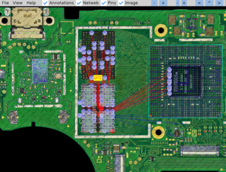
As electronics have advanced, they’ve not only gotten more powerful but smaller as well. This size is great for portability and speed but can make things like repair more inaccessible to those of us with only a simple soldering iron. Even simply figuring out what modern PCBs do is beyond most of our abilities due to the shrinking sizes. Thankfully, however, [μSoldering] has spent their career around state-of-the-art soldering equipment working on intricate PCBs with tiny surface-mount components and was just the person to document a complete netlist of the Nintendo Switch through meticulous testing, a special camera, and the use of a lot of very small wires.