
![hacker-tactic:-single-pcb-panels-[hackaday]](https://i0.wp.com/upmytech.com/wp-content/uploads/2024/07/195947-hacker-tactic-single-pcb-panels-hackaday.jpg?resize=800%2C445&ssl=1)
Hacker Tactic: Single-PCB Panels [Hackaday]
Ordering a PCB? Two of them? Three? Five? For about eight years now, I’ve been regularly ordering large numbers of different PCBs, and, naturally, have developed a toolkit to make things smoother. One trick is PCB panelization, and you should really know about it.
You might’ve encountered PCB panels already. Perhaps, if you order PCBA at a fab, you will get your board returned in a whole new form-factor, with rails on the sides that you have to snap off before your PCB is usable. Those rails are used so that your PCBs are easier to handle during assembly, but that’s far from the only reason why you would make a panel.
If you need multiple pieces of a PCB, your fab may say that building 50 pcs is classified as “large batch” and that takes longer than 30 days, which delays your entire PCB order. I’ve been there, five years ago, running out of time right before Chinese New Year. The fix was simple – I made a 2×2 panel and ordered that in quantity of 10-15. Panelization might be a little more expensive, or maybe even cheaper, but, most importantly, it will be faster.
In a few hours’ time, I sat down, figured out that KiCad has built-in features for panelization, and ordered panels instead of separate PCBs. Thanks to that, I made the Chinese New Year deadline that year and could successfully restock my store, letting me earn a fair bit of money instead of keeping a popular product out-of-stock – ultimately, helping my family stay up on rent that month.
Panelization lets you hack around many PCB ordering and assembly limitations, and I’ve only gotten started – there’s way way more! For now, let’s sort out panelizing multiples of the same PCB. As long as your boards are using KiCad (or KiCad-converted from Eagle/EasyEDA/Altium/gerbers), there’s no better software than KiKit.
KiKit Simply Rules
KiKit is a KiCad plugin by [Jan Mrazek], and it’s had a ton of work put into it to make it a one-stop shop for KiCad panelization. Once installed, KiKit lets you do panelization from inside KiCad, with a nice GUI that lets you define all sorts of parameters. Install it and go wild. KiKit is a little tricky to install and there’s some slightly uncomfortable behaviour – in other words, just like the majority of the software we use, but it brings you massive benefits for some possible initial pain.
Open an empty board by opening pcbnew (PCB Editor) standalone, then, in the top toolbar, press the KiKit button on the right. Pick a board in “Input”, click “Output” and enter something like panel.kicad_pcb, set rows and cols to something like 2 and 3, hspace and vspace to 2mm, set Cuts=>type to mousebites, and press Panelize in the right bottom corner.
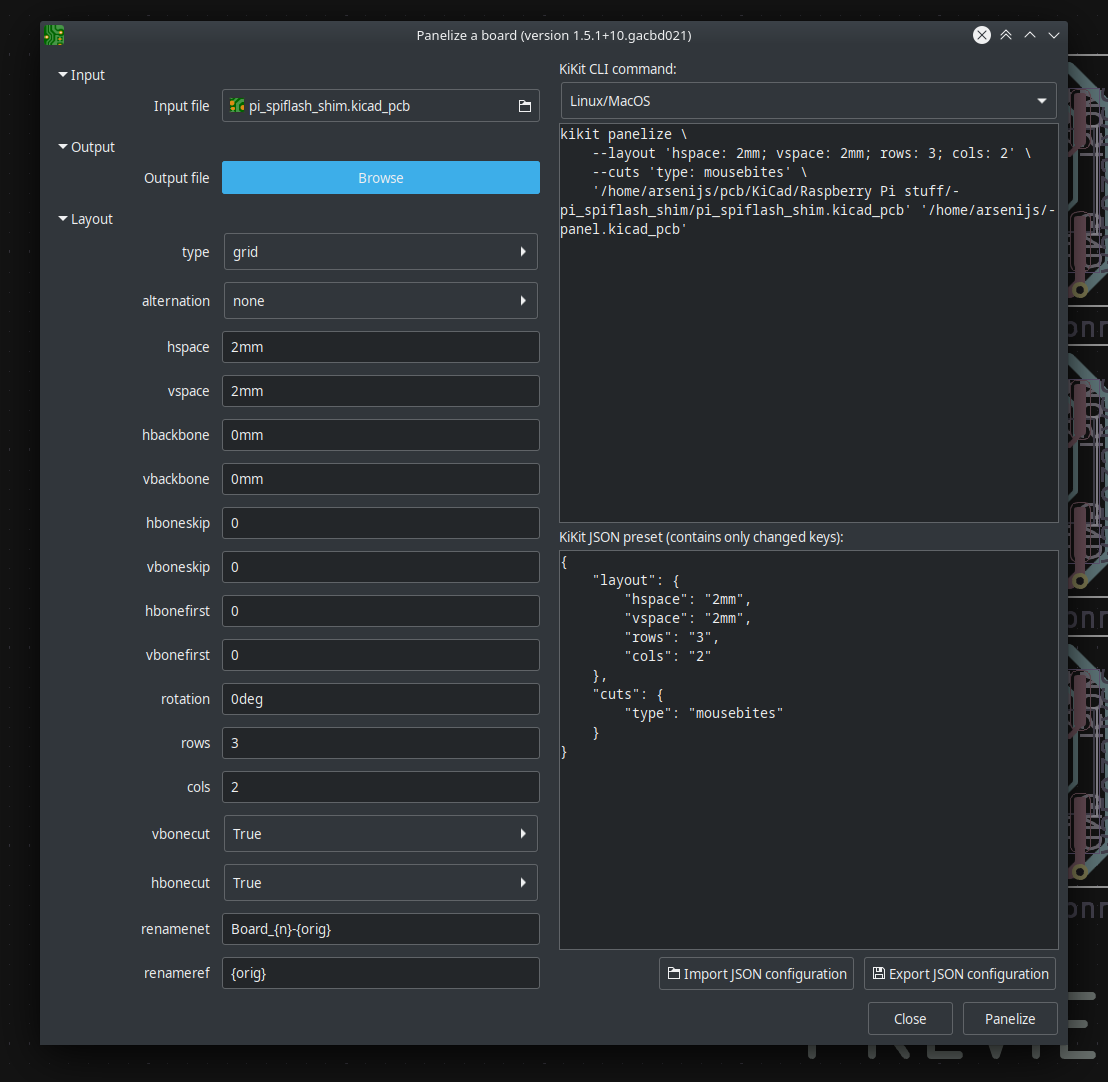
This is the most basic panel you could do, and if you ever have had to draw such a panel manually, you will notice that this just saved you a ton of work. This panel has no fiducials, no outer frame, no V-cuts, but all of these are just a couple dropdowns and digit fields away. Want to order a large number of PCBs? This is how you do it, and there’s a good few uses for this. One of them for me used to be decreasing prices at JLCPCB, but as they ramped prices up over the years, this benefit has faded – another PCB fabs might still give lower prices for panels for you, however, so watch out. There’s other uses that remain true, too.
Panels So Nice To Handle
I designed a large-ish capacitive touch panel a couple years ago, a pandemic-related project that would help mark your attendance of something like a hackerspace. It used a custom touch controller and giant electrodes: 2 cm x 2 cm PCBs with rounded edges. I wanted to have a dozen kits of them, which would’ve led to a batch size of 200 and increased production time that’d delay my entire order.
Instead of ordering 200 of a single PCB, I made 4×4 panels. They were way cheaper, quick to manufacture, and way easier to manage once received. I wanted to mail them out to some hackerspaces, and the panels also helped – instead of counting out 16 of them and then having them rattle around in an envelope, I could take a single panel and throw it into the package. A cherry on top is that your PCB’s recipient gets the satisfying task of splitting a V-cut panel into separate PCBs, too.
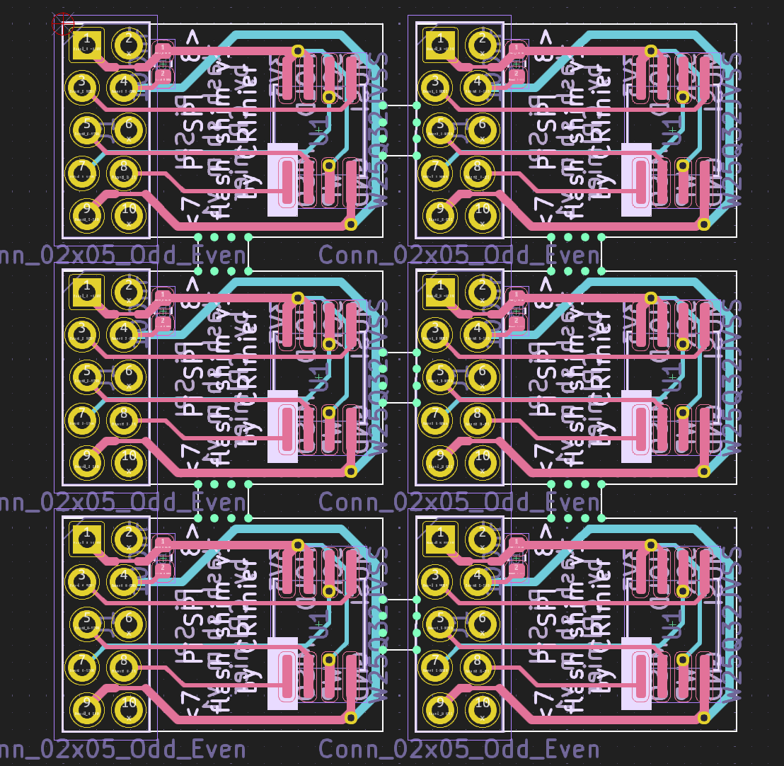
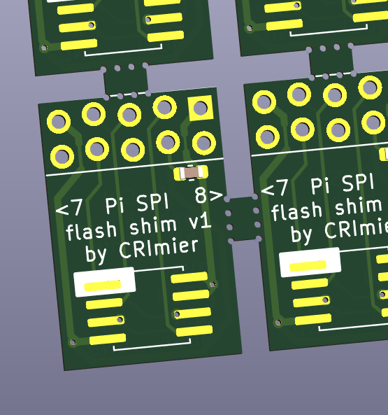
Here’s another example from the PCB design above. It’s a shim for a Linux-powered Raspberry Pi that lets you program SPI flash chips with the standard “SPI flash” pinout – SOIC-8, SOIC-8W, and DFN. With this shim, you don’t need to carefully match jumper wires – just desolder the chip in question, solder it onto the shim aided by elongated pads, then plug the shim onto a Pi header; it will hold onto the Pi GPIO header pins and make electrical contact thanks to staggered holes.
There’s more, of course – once you scale up a project of yours, you can easily do manufacturing with these, and, again, save a fair bit of money!
The Fab Wanted It, So I Improvised
For manufacturing, it’s common that your board needs a panel around it; specifically, a thin PCB frame with the board held inside by mousebite, with perhaps even on-frame fiducials for assembly positioning. This makes your possibly-unorthodox-shape board into a panel that an assembly house workers and their machinery can easily handle. Sometimes you can have the fab handle the panel stuff, but some assembly houses will want you to mail your files already prepared, rail added and all. KiKit makes such panels a breeze, as you might guess.
panel.json for this specific panelOnce again, you can save a fair bit of money if you make such a panel. Take JLCPCB’s “economic” tier PCB assembly service – it’s notably cheaper than “standard”, but it has limitations on what you can do. For instance, you have to pick from a list of allowed PCB thicknesses and soldermask colours. I needed two-layer 1 mm thick black PCBs, but I wanted like 50 of them where economic assembly would only allow 30. On this board, having to use “standard” assembly would be a significant price jump with no benefit at all.
Instead, I made the PCB into 1 x 2 panels with KiKit and ordered 30 panels – each panel counts as a PCB for PCBA purposes. This let me order 60 pcs of an assembled PCB significantly cheaper, at the cost of some depaneling once the boards arrive, which, again, that’s just a fun thing to do. JLCPCB might clamp down on this and force you to use more expensive assembly, but, for now, you can easily fab 150 pcs of a small PCB while still keeping within economic assembly tier.
Once you’ve defined the frame for the PCB, KiKit will have some JSON that defines your panel’s parameters. Don’t just close the PCB editor you’ve been KiKit’ing in! Exporting KiKit’s JSON is vital, unless you want to re-configure the parameters every time you need to regenerate the panel; I usually save it as panel.json in the folder where the board file is. In fact, there should really be an autosave option – anyone up to do a pull request?
Naturally, with KiKit boards, you can easily export pick and place data – the end result is just a KiCad board, you can even edit it afterwards. I typically use a fab-aimed plugin when ordering PCBA, but you can also just export .pos and .csv BOM files the same way you would from any other KiCad PCB.
Tips And Tricks
V-cuts are pretty clean to handle: you just snap the boards apart. Mousebites are perhaps less so because they leave jagged edges on the PCB. Watch out here – using sandpaper on the edges is not the greatest idea, with this dust being both carcinogenic and abrasive. The resulting dust is going to go everywhere, it’s irritating in a literal sense, and you might even end up having to wash it off your PCBs. Instead, try using a box cutter with those snap-off blade sections, sliding it against the board outline – it should be able to cut off the jagged edges, leaving no dust, just slices of where mousebite remains used to be.
As a footnote, here’s a tactic I want to try out – using V-Cuts for making castellated modules on the cheap. I don’t want to pay a significantly higher price for a special castellated process, but I still want to PBCA like 100 pcs of a cool small module so I can throw it into postal envelopes and put it on my products; also, V-Cuts feels like you’d get nicer plated edges than milled. I don’t know if a fab would accept it, but this article says it’d be okay to do and such holes can work as inter-board interconnects. I’m out to try this trick out soon, and will report back!
We’ve panelized a single PCB today – which is cool and helpful, but there are even more exciting options. Next time, I’m going to show you how to save even more money and maybe make assembly even quicker, as well as save a fair bit on SMT stencils – stay tuned!