
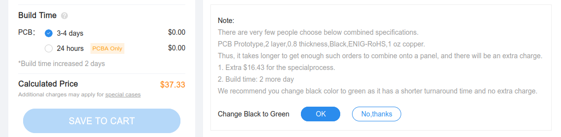
![hacker-tactic:-multi-design-panels-[hackaday]](https://i0.wp.com/upmytech.com/wp-content/uploads/2024/07/199738-hacker-tactic-multi-design-panels-hackaday-scaled.jpg?resize=800%2C445&ssl=1)
Hacker Tactic: Multi-Design Panels [Hackaday]
Last time, we talked about single-PCB-design panels, all the cool aspects of it, including some cost savings and handling convenience. Naturally, you might wonder, and many did – can you put multiple different PCBs on a single panel? The answer is “yes, without a doubt!” The tool we used last time, KiKit, will not be as helpful here, so we’ll be looking elsewhere.
Making multi-PCB panels can help you save money, naturally, but it can also make your assembly a whole lot easier, and it can bring you hacking to a whole new level. It sure helped with mine! You might have already learned that some fabs scoff at multi-design panels and add surcharges. Well, you’ll be delighted to learn that there are more hacker-friendly fabs out there, too.
Developing PCBs In Bulk
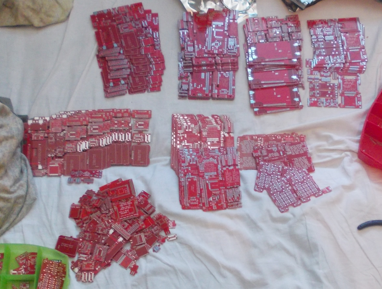
So far, I’ve worked on about 300 different PCB designs, with half of them available in my monorepo. I’ve assembled and tested just about half of these. You might guess that this would cost a lot of money, and that assembly would take a fair bit of time, but I have some tricks up my sleeve. For a start, you can easily order PCBs 10-12 times more cheaply if you do multi-panel.
Around 2016, I decided to start developing PCBs in larger quantities, both fully-featured device PCBs and small building-block boards for all sorts of mods. I was trying to do this on a pretty tiny budget. It helped that I started working on ZeroPhone soon after, a smartphone you could mod with custom PCBs, and there were more than enough different mods to get creative with. In a month’s time, I could easily develop a dozen PCB designs, and the trick to that was knowing a friendly PCB service.
How do you order PCBs in large quantities on a budget? As long as you keep to two-layer boards, it turns out you can combine these PCBs into a panel and order that panel from a service like DirtyPCBs. DirtyPCBs is a hacker-friendly PCB service with flat prices, no sudden charges for unpopular options, and zero extra fees for different design panels. The trick is that you just need to make them in a manufacturable way.
This is a notable contrast to most other fabs, which will require extra fees for every deviation from the norm. This is counterproductive and an impediment to creativity when you’re offering a service to hackers. The ability to experiment without being financially punished for it is an important one, but many fabs will see different-design panelization fees as an attempt at cheating them out of money, as opposed to a hack you can do to make your life easier in a dozen different ways.
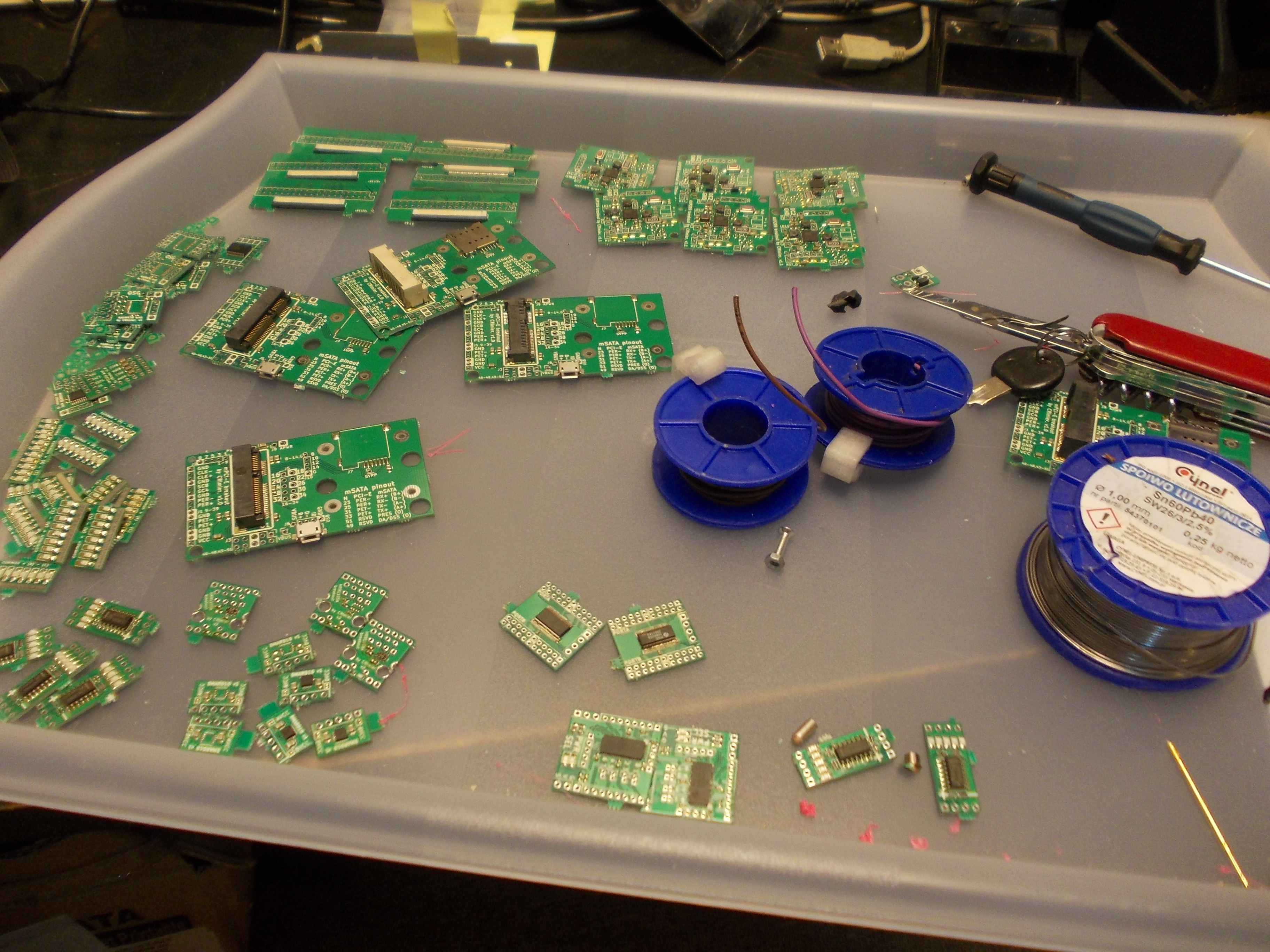
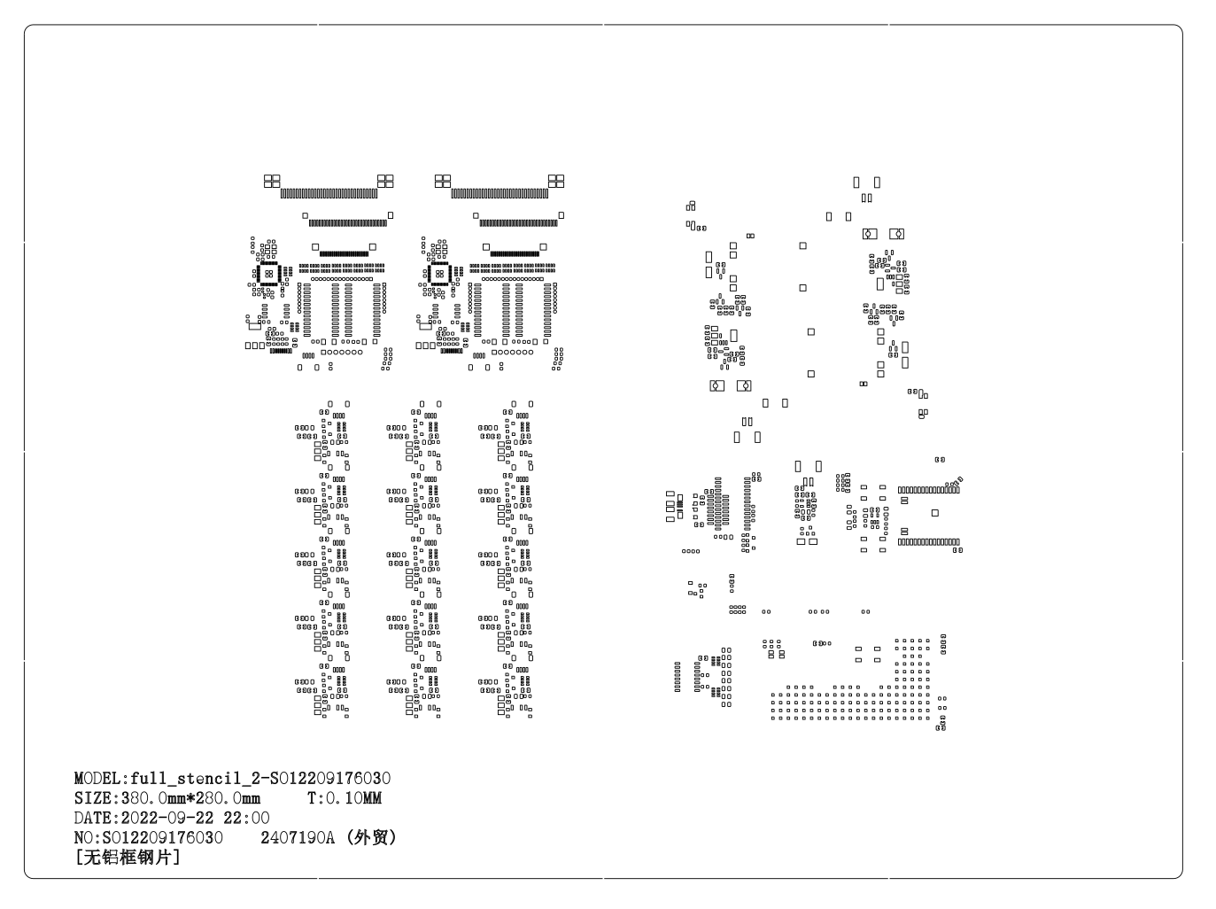
Just like with single-design panels, multi-design panels are easier to handle than an assortment of transparent baggies with PCBs – it’s a single PCB until you break it apart, which in itself is a pretty satisfying process. They’re also easier to assemble en masse, because you can stencil them all together.
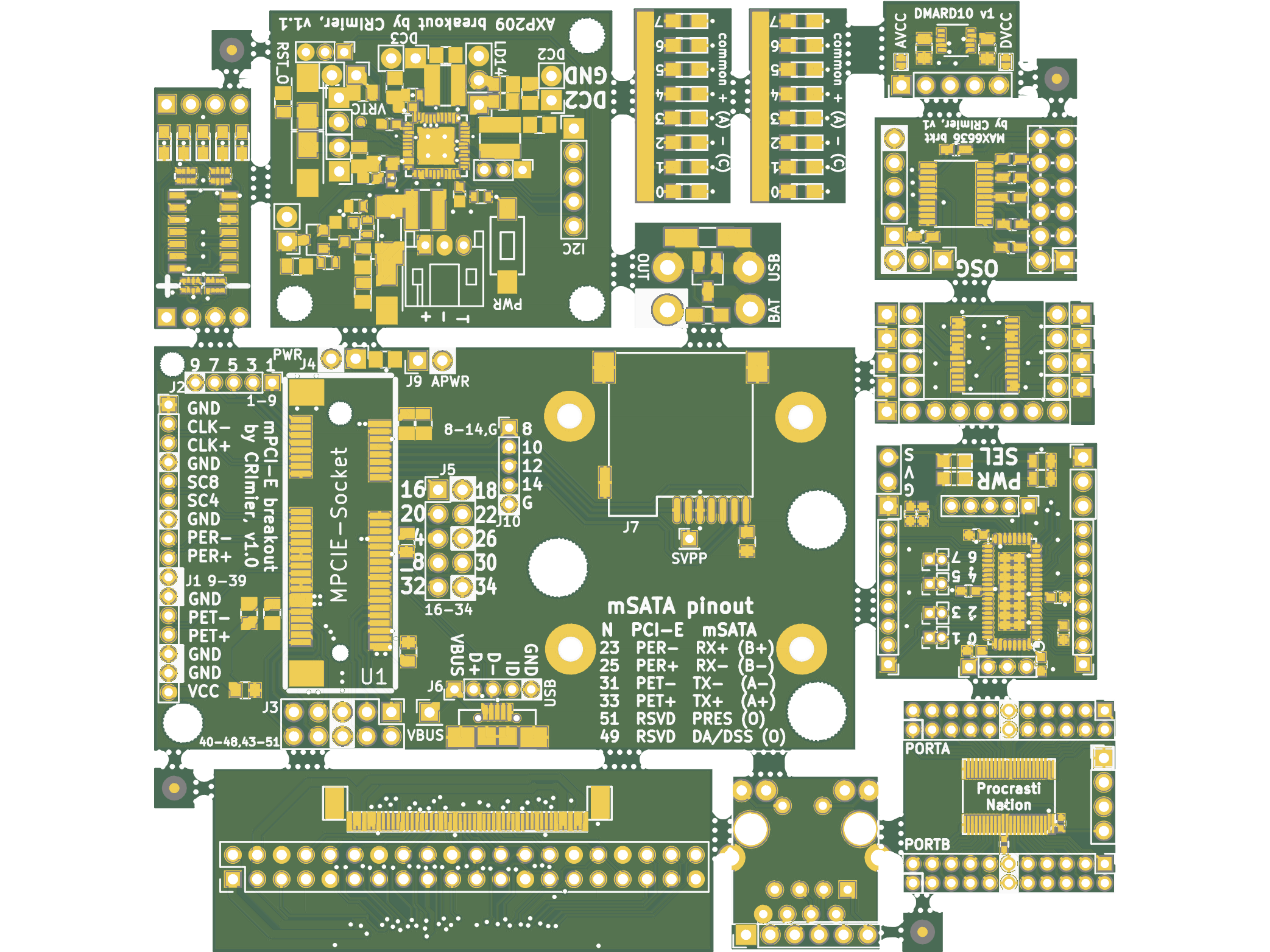
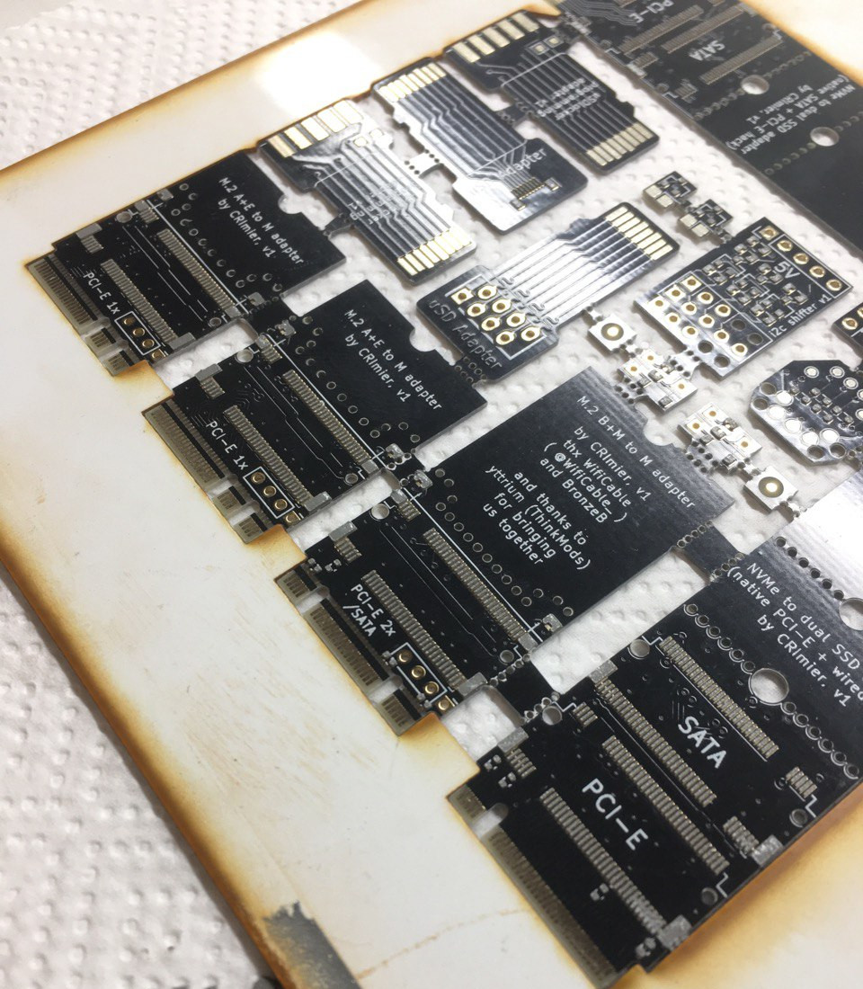
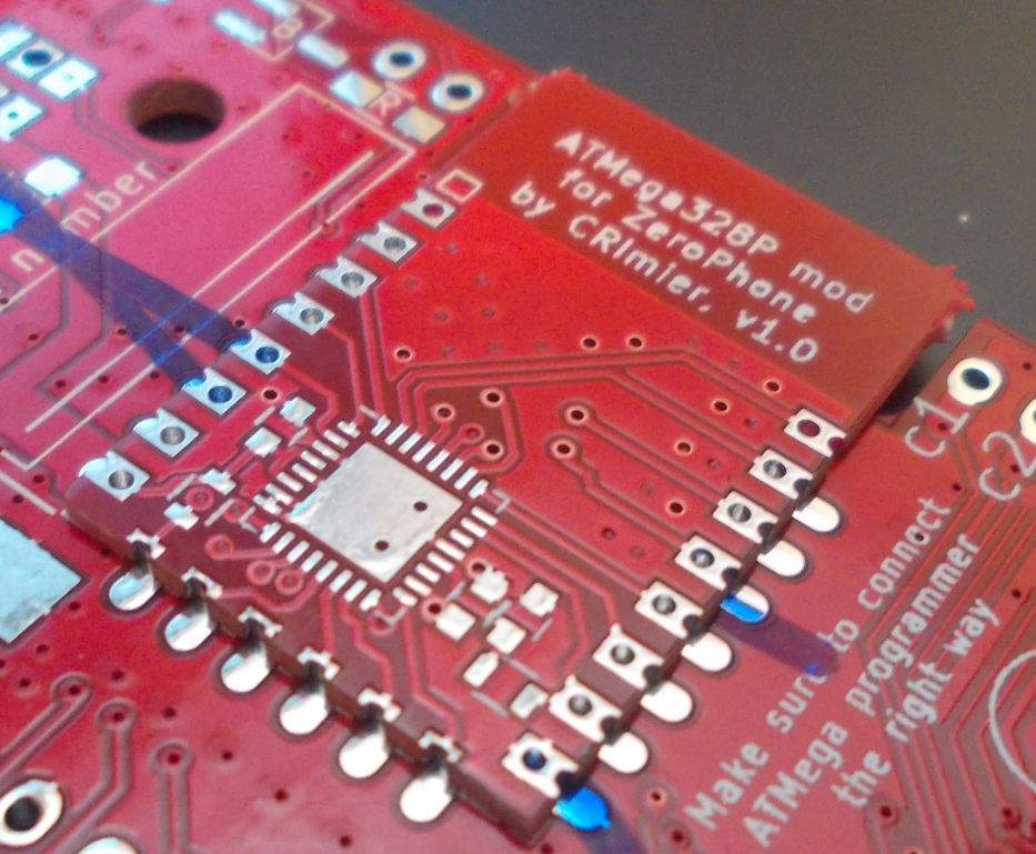
Look at the picture to the left – these PCBs on the bottom might look simple, but the M.2 sockets are a bother to solder, and you really want to stencil them, because each pasting pass takes time. If I do a panel like this in one shot, I only need a single swipe of an old credit card with a line of solder paste, and I can mount five M.2 slots at once – then hot air them all at once quickly, or pop them into a reflow oven.
This makes assembly way, way easier, and it doesn’t stop here! I’ve noticed something outstanding – the assemble-full-panel-at-once process has actually motivated me to finish even the smallest projects, making sure my bare PCBs always get components soldered onto them. This left me to just bringup or test them at some point, which is tempting and fun – as opposed to assembling an individual board piece by piece, which can feel tedious. Before that, I would assemble projects individually, and it was quite easy to just never assemble a board, leaving a project forever incomplete. I haven’t been ordering panels for a bit now, and having written this, next month I just might do it again, because I realize that I really miss it.
As some of you might guess, this also helps with at-home pick and place, letting you skip the per-PCB setup time and making it even easier to assemble your projects than before. I’ve used a pick and place machine for assembling quite a few of these panels, and for that, I wrote a script combining all .kicad_pos data into a full panel’s .kicad_pos. I haven’t updated it in a fair bit, and it might have hiccups handling the bottom layer board rotations, purely through my lack of testing, but it’s still a large timesaver if you got a PnP handy. Over time, I learned to flip my boards in a way that the “most SMDs” side is the top side on the panel – this will save you a large amount of time if you’re using pick and place or even just stenciling such a panel, especially if you account for the effort of making a custom jig for stenciling a PCB with components mounted to its bottom.
Show Me the Money
I’ve done ESP-12 style drop-in replacement modules with quick-and-dirty castellations, a test board I wanted to make in the cheapest possible way as a proof of concept, and it came out well for what it was. With someone like JLCPCB, I would’ve gotten at least an attempt to upsell me on their (seriously expensive) castellations, and at worst, a requirement to have me remake my board entirely, something I’ve had to deal with recently. And at DirtyPCBs, I could pick any colour I wanted. At some point, I used different colours to denote “generations” of my designs; to this day, if I see a blue PCB at home, I know it’s from about 2018, and a red PCB is from around 2020.
Of course, this is for two-layer boards, but many of our designs can fit in two layers – as I keep demonstrating in the design review series. Also, a much-needed detour on manufacturability! You need to make sure that the PCBs in your panels are connected well to each other, so that the individual boards don’t fall out of your panel during manufacturing or flying probe test – this is important. DirtyPCBs also asks us that you add rails on all four sides, ideally; you can do V-Cuts for those. You don’t get a special castellation process either, but you can do V-Cuts with the usual “put straight lines cutting across the board on your Edge.Cuts” trick; all V-cuts must be at least 7 cm long, a standard requirement for fabs. Keep the distances between boards to 2 mm or more so that the outline can be milled well, and make sure to thoroughly read DirtyPCBs’ ordering requirements; the more professional you are with compiling your panels, the smoother your ordering experience will be.
I usually order 10 cm x 10 cm panels, each full of boards of various kinds, and it’s pretty fun to put them together. Ask your friends if they have some boards they wanted to order, perhaps do a PCB design weekend, add them to your panels, and, suddenly, you’ve started a mini-OSHpark! Boost this by giving your friends design review or even assemble their boards, and, all of a sudden, you find yourself in the middle of a hacker community.
Multi-design panels are cheaper, they make your assembly easier, help you advance your projects, work around fab limitations, or even put your hackerspace or hacker collective closer together. If a design is larger than 10 cm x 10 cm or has more than two layers, I go for one of the usual suspects, but there’s a number of designs I will only ever order in panels. Now, let’s take a look at how you put a multi-design panel together.
Putting It All Together
Once the PCBs arrive, here’s the best part yet. You can assemble this kind of panel all at once, too! Again, make sure your boards are all flipped so that all component-bearing sides are on the same side, and you can stencil, assemble, and bake such a panel in one go. As I’ve shown, this is how I’ve managed to design a good few M.2 cards and other boards on the cheap – stenciling a single M.2 card at a time is bothersome, but stenciling seven at once is pretty comfortable.
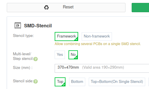
For stenciling, you’ll want a stencil, naturally – DirtyPCBs built-in option is pretty competitive, and the stencil you get is of a comfortable size. I used to order stencils for these panels on JLCPCB, but recently, JLC changed their policies and multi-design stencils are no longer the same price as single-design ones, with steep extra fees. So, now JLC stencils are not affordable in the slightest – but PCBWay still explicitly allows multi-design stencils for no cost increase, so it might be a better option.
Even if you decide to order a custom-sized small stencil that fits into a standard JLCPCB mailing box, JLCPCB hits you with a hard-to-notice 300 g weight addition to your order for what’s just a paper thin piece of aluminium in a ziplock bag – the cheap stencils are actually paid for by hidden “shipping” fees, so, don’t focus on the $7 stencil price point too much. If you’re ordering a lot of designs, say, for a group of people, as I do sometimes, combining DirtyPCBs for 10 v cm x 10 cm two-layer panels and some other fab for everything else including stencils is probably the most cost-effective option.
For all the panels shown above, I used GerberPanelizer from ThisIsNotRocketScience, a software that we’ve covered on Hackaday before. This one is Windows-only, hasn’t had a release for a while and the last binaries are from 2020, which are no longer compatible with KiCad 6 or beyond, but the state of newer-than-2020 code on GitHub is pretty good.
Here is my workaround: install Visual Studio Community onto a Windows VM, load the Visual Studio project included in the repo, pick the GerberPanelizer project, compile it and use the .exes generated. Drag and drop boards into a GerberPanelizer window, add tabs with T, remember to save your project (File=>Save) before you export it so you can re-export it later on if you decide to make a small change to one of the boards, and generate the gerbers.
Want a Linux alternative? You might try and run GerberPanelizer on Linux, as multiple people on GitHub have tried to varying degrees of success; alternatively, you could try out this software that claims Linux support. I haven’t checked this one out yet, but it seems good, and I might try it out when I finally get way too tired to work with Windows 10’s endless nuances. If you have recommendations, we’re all ears!
Do you want to order stencils for cheaper? If so, you might be happy to learn that multi-design stencils are a thing; about the only issue is that you’ll be expected to cut the stencils apart yourself – remember to use scissors that you don’t care about, and tape the stencil edges with painters tape afterwards. (You should be doing that anyway, they will cut you when you least expect it.) Doing multi-design panels and want stencils for these? You can use the panel gerber output files as input to the GerberPanelizer and combine them with other boards, of course, creating a multi-multi-PCB stencil.
How do you compile such a stencil panel? For a start, you can simply use KiCad – as long as all your boards are all made in KiCad, or you simply import them into KiCad for a stencil panel’s sake. Open the PCB editor in standalone mode, use File=>Append board to add all your boards in there, then export gerbers like you normally would. You can’t quite use this for making PCB panels easily, sadly, because adding mousebites manually is kind of a pain, so unless all your boards are the same size and you can do V-cuts, you’ll want to use a suite like GerberPanelizer.
There’s a lot to explore to the multi-panel technique, so you better keep it in mind – when you’re planning a multi-design project, doing something like making a PCB case out of PCBs, or just looking to do a PCB design weekend marathon turning every single of your circuit building blocks into a breakout, multi-design panelization will likely save you a bunch of money and trouble.