
![design-review:-switching-regulator-edition-[hackaday]](https://i0.wp.com/upmytech.com/wp-content/uploads/2024/06/190274-design-review-switching-regulator-edition-hackaday-scaled.jpg?resize=800%2C445&ssl=1)
Design Review: Switching Regulator Edition [Hackaday]

This article was prompted by a friend of mine asking for help on a board with an ESP32 heart. The board outputs 2.1 V instead of 3.3 V, and it doesn’t seem like incorrectly calculated feedback resistors are to blame – let’s take a look at the layout. Then, let’s also take a look at a recently sent in design review entry, based on an IC that looks perfect for all your portable Raspberry Pi needs!
What Could Have Gone Wrong?
Here’s the board in all its two-layer glory. This is the kind of board you can use to drive 5 V or 12 V Neopixel strips with a firmware like WLED – exactly the kind of gadget you’ll want to use for LED strip experiments! 3.3 V power is provided by a Texas Instruments TPS54308 IC, and it’s the one misfiring, so let’s take a look.
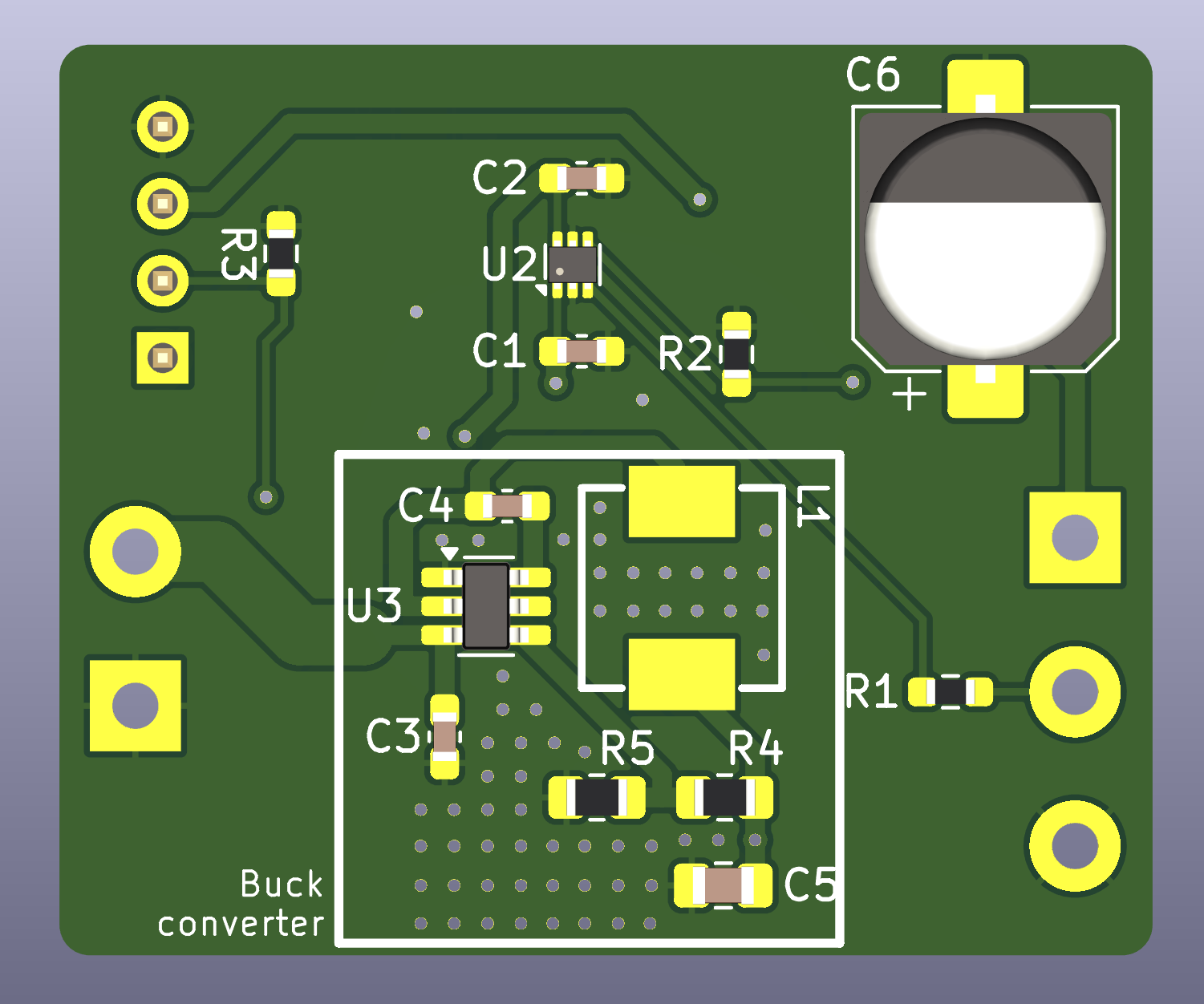
The design has an ESP32 on the opposite side of the switching regulator. For review purposes, let’s pull the regulator circuit out – disable all front layers (copper, silk, mask, courtyard and paste), hide vias, then box select the regulator circuit and move it out. I’ve also added net labels to the circuit – here’s a screenshot.
Furthermore, from the pinout and also the layout recommendations, it appears this regulator is designed in a way that all switching circuitry can be. Yet, this design has the inductor go all the way to supposedly sensitive side. Thankfully, this is easy to fix.
Refresher – FB and SW traces have to be as short as possible, inductor as close to SW as possible, and the VOUT to FB connection can be a separate tracks on the other layer. With that in mind, let’s move the inductor to the other side of the regulator, move the FB resistors to the FB pin, and see how far we get.
My Take Versus TI’s Recommendation
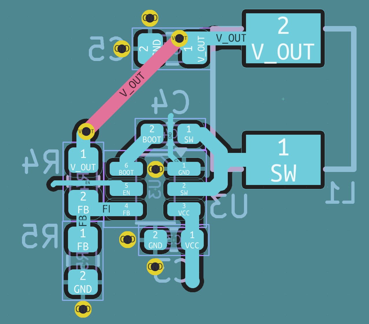
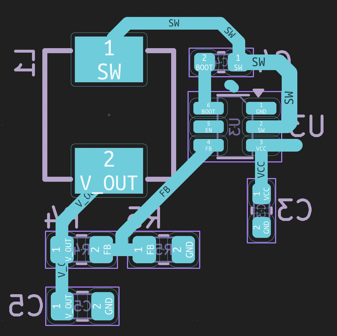
Since this is a TI chip, it also has a diagram for the layout recommendation! Let’s take a look how far off the mark we are, and it appears we aren’t that far. Curiously, it wants us to put SW onto another layer. Having switching current pass through extra inductance doesn’t sit right with me, personally, but my guess is that they want to minimize switching current flowing under the regulator, as the recommendation suggests.
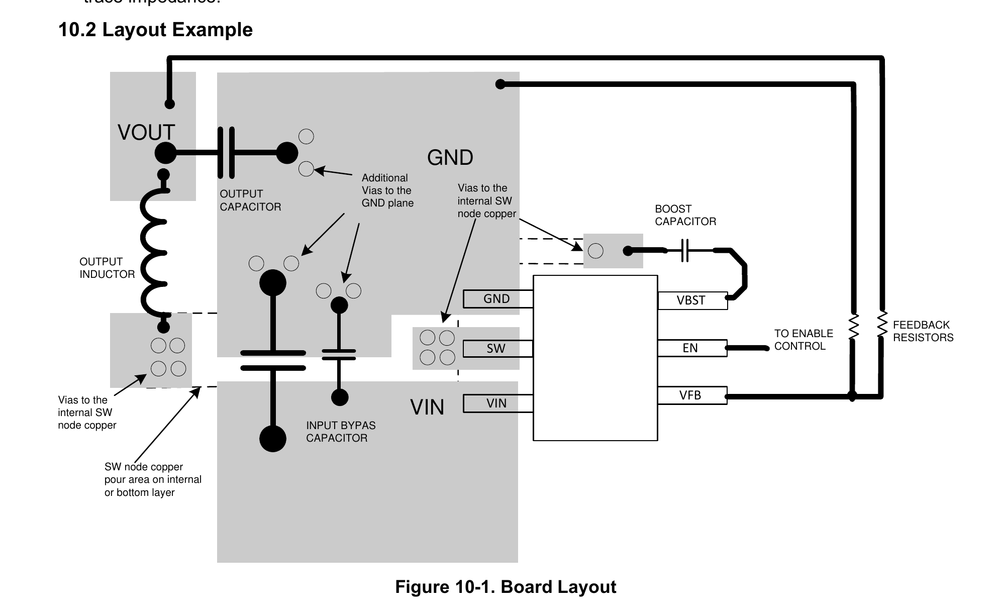
Another part that’s curious to me, is a suggestion for a Kelvin connection for the FB net’s GND pin. TI also publishes data for evaluation boards, and the TPS54308 has such a board indeed. Seeing on the page 13 of the evaluation board datasheet, I’m not quite seeing a Kelvin connection, unless Kelvin is the name of the engineer involved in designing the board. I do see that GND is tapped with a via far away from the area where switching happens, so it might just be that.
At this point, I’m curious whether my take is a dealbreaker, but since TI’s recommendations are available, I might just end up implementing exactly that and sending the files back. So, we take this circuit, implant it back into the board, order a new revision, and keep our fingers crossed.
A Pi-suited UPS, On A Stamp
A week ago, [Lukilukeskywalker] has shared a board with us, asking for a design review. The board is a stamp that houses a LTC4040 chip, and the chip itself is a treat. It takes 5 V, outputs 5 V, and when connected, it generates 5 V from a battery. It supports both regular LiIon, can do up to 2.5 A, and appears to be a perfect option if you want to power a Raspberry Pi or any other 5 V-powered SBC on the go.
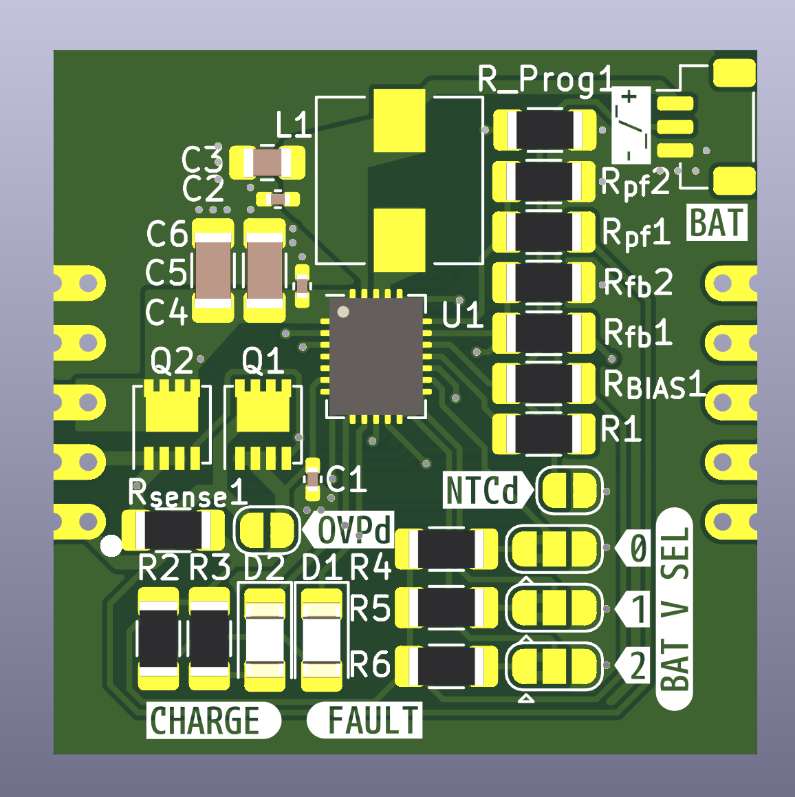
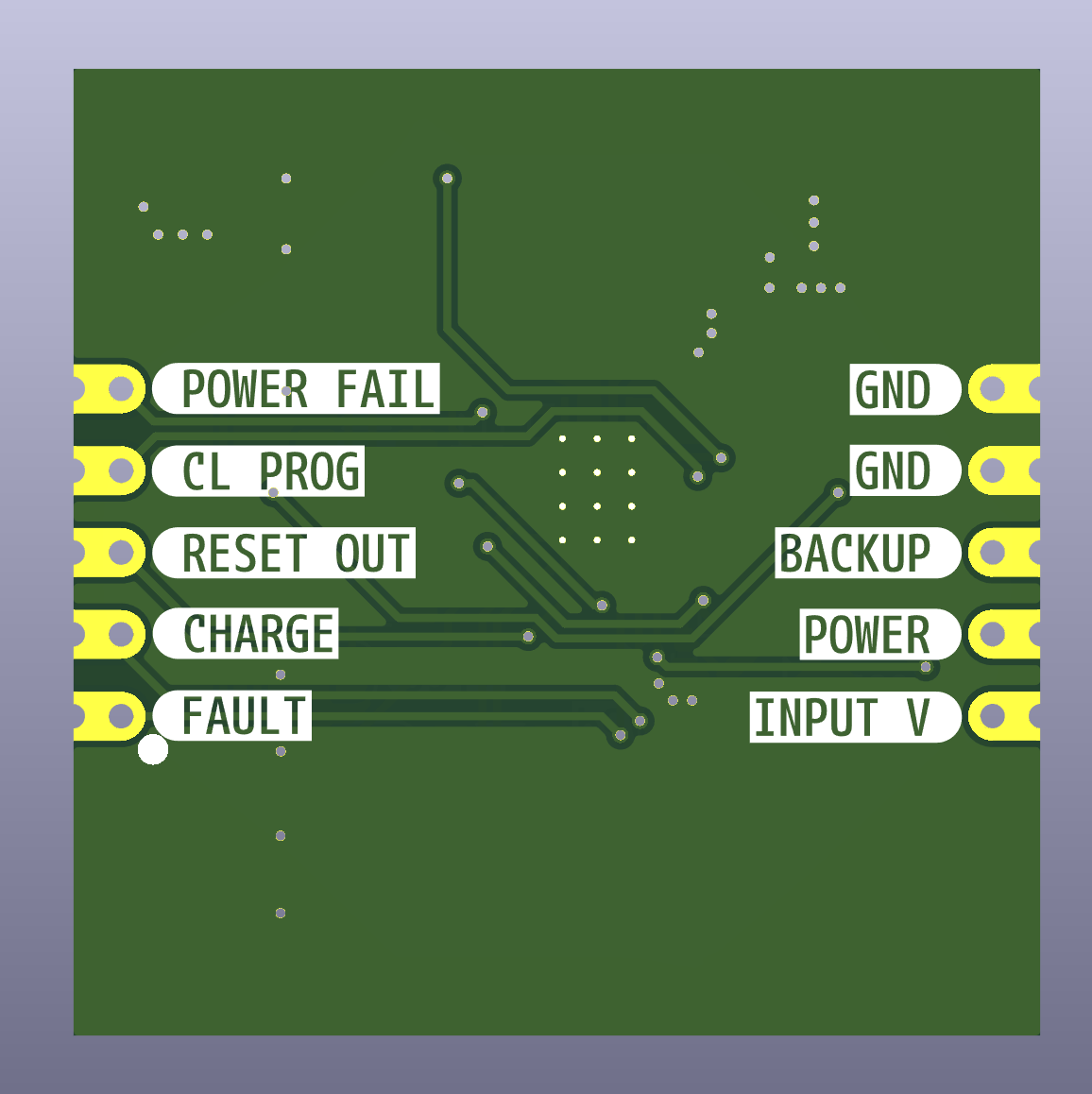
There are a few small nits to pick on this board. For instance, the connector for the battery is JST-SH, 3-pin, with one pin for BATT+. 2.5 A at 5 V means 12.5 W means up to 4 A at 3.5 V battery level, which might just melt a JST-SH connector or the gauge of wire you can attach to a JST-SH-sized metal contact. However, it’s switching regulator time, so let’s take a look at that specifically.
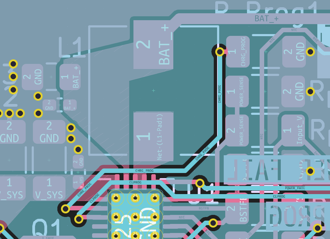
Well, there are only two tracks that really interrupt the switching path above them, and both could be moved to the left. One of them is for a resistor that sets the charging current limit, and another goes to a castellated pad. Moving the latter is going to break the symmetry, but remember – it’s okay for a stamp to be asymmetric, that helps you ensure it’s mounted on your board correctly!
Sadly, while Linear Tech makes fancy tech, their evaluation board data isn’t as available as TI’s – there’s a PDF with schematics, but no layout data I could find. However, comparing to the pictures, you can see that the general layout of the switching area is correct, our hacker correctly uses polygons, the feedback circuit is pretty nice – it’s just these two tracks that are a bit uncouth when it comes to the switching regulator part of it. As for reviewing the rest of the board, you can read this article!
Towards A Powerful Future
Got switching regulator designs that didn’t quite work right when you put them to test, or that you’re yet to order and feel cautious about? Show them to us down below in the comments, and let’s take a look; your circuits deserve to operate at their best capacity possible.
And, as usual, if you would like a design review for your board, submit a tip to us with [design review] in the title, linking to your board files. KiCad design files strongly preferred, both repository-stored files (GitHub/GitLab/etc) and shady Google Drive/Dropbox/etc .zip links are accepted.