
![an-open-source-6kw-gan-motor-controller-[hackaday]](https://i0.wp.com/upmytech.com/wp-content/uploads/2024/08/205656-an-open-source-6kw-gan-motor-controller-hackaday.png?resize=800%2C445&ssl=1)
An Open Source 6kW GaN Motor Controller [Hackaday]
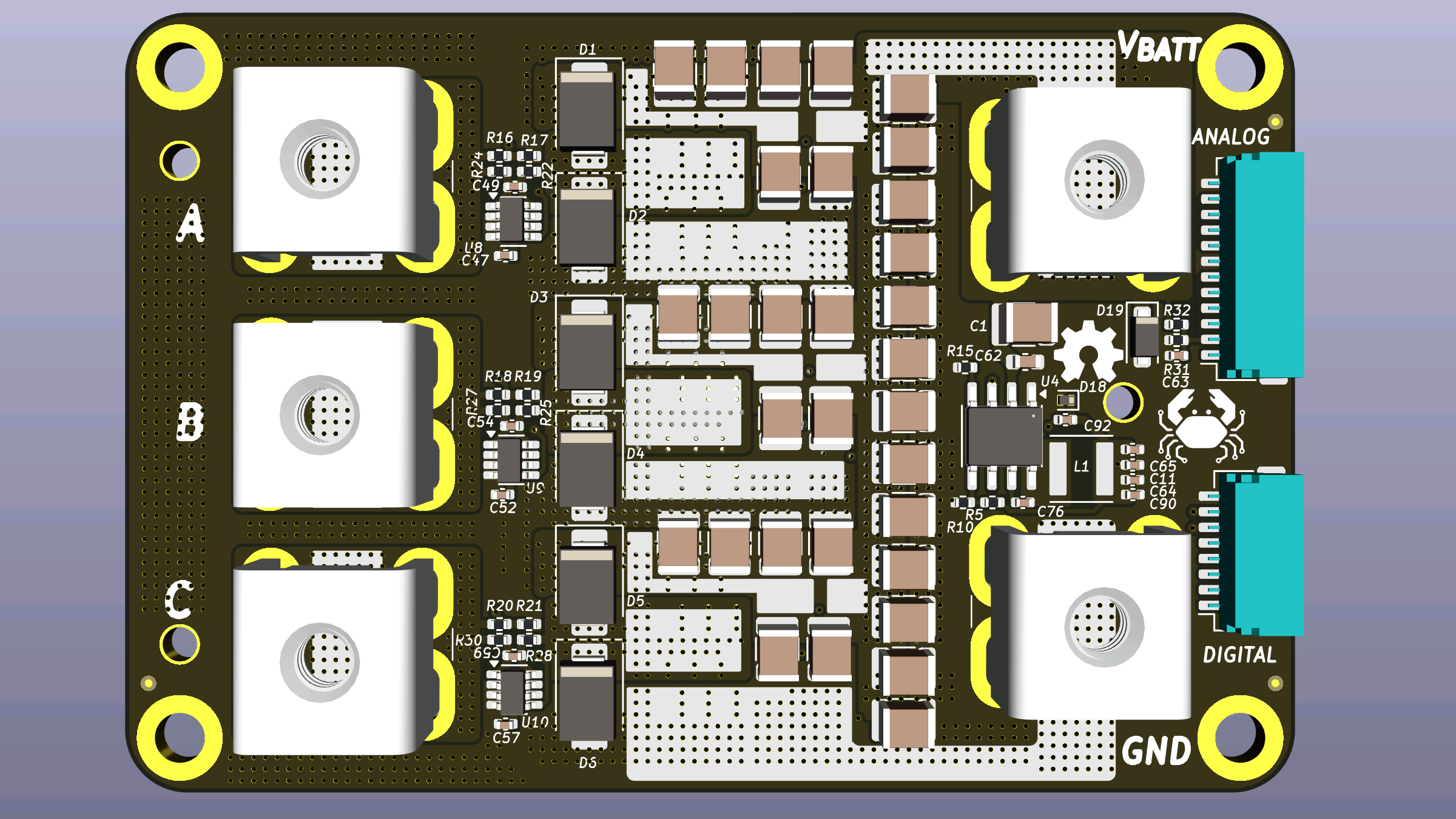
We don’t know how you feel when designing hardware, but we get uncomfortable at the extremes. High voltage or current, low noise figures, or extreme frequencies make us nervous. [Orion Serup] from CrabLabs has been turning up a few of those variables and has created a fairly beefy 3-phase motor driver using GaN technology that can operate up to 80V at 70A. GaN semiconductors are a newer technology that enables greater power handling in smaller packages than seems possible, thanks to high electron mobility and thermal conductivity in the material compared to silicon.
The KiCAD schematic shows a typical high-power driver configuration, broken down into a gate pre-driver, the driver itself, and the following current and voltage sense sub-circuits. As is typical with high-power drivers, these operate in a half-bridge configuration with identical N-channel GaN transistors (specifically part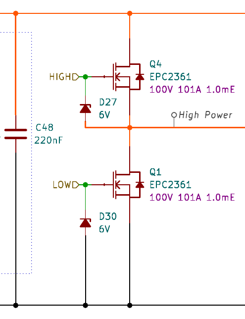
The design uses the LM1025 low-side driver chip for this task, as you’d be hard-pushed to drive a GaN transistor with discrete components! You may be surprised that the half-bridge driver uses a pair of N-channel devices, not a symmetric P and N arrangement, as you might use to drive a low-power DC motor. This is simply because, at these power levels, P-channel devices are a rarity.
Why are P-channel devices rare? N-channel devices utilise electrons as the majority charge carrier, but P-channel devices utilise holes, and the mobility of holes in GaN is very low compared to that of electrons, resulting in much worse ON-resistance in a P-channel and, as a consequence, limited performance. That’s why you rarely see P-channel devices in a circuit like this.
Of course, schematic details are only part of the problem. High-power design at the PCB level also requires careful consideration. As seen from the project images, this involves heavy, thick copper traces on two or more heavily via-stitched layers to maximise copper volume and lower resistance as far as possible. But, you can overdo this and end up with too much inductance in critical areas, quickly killing many high-power devices. Another vital area is the footprint design for the GaN device and how it connects to the rest of the circuit. Get this wrong or mess up the soldering, and you can quickly end up with a much worse performance!
We’ve seen DIY high-power controllers here a few times. Here’s an EV controller that uses discrete power modules. Another design we saw a few years ago drives IGBTs for a power output of 90kW.