
![a-simple-guide-to-rf-pcb-design-[hackaday]](https://i0.wp.com/upmytech.com/wp-content/uploads/2024/08/206845-a-simple-guide-to-rf-pcb-design-hackaday.png?resize=800%2C445&ssl=1)
A Simple Guide to RF PCB Design [Hackaday]
[Hans Rosenberg] knows a thing or two about RF PCB design and has provided a three-part video demonstration of some solid rules of thumb. We will cover the first part here, and leave the other two for the more interested readers!
The design process begins with a schematic diagram, assuming ideal conductors. Advanced software tools can extract the resistive, inductive, and capacitive elements of the physical wiring to create a parasitic model that can be compared to the desired schematic. The RF designer’s task is to optimize the layout to minimize differences and achieve the best performance to meet the design goals. However, what do you do when you don’t have access to such software?
[Hans] explains that at low frequencies, return current flows through all paths, with the lowest resistance path taking most of the current. At higher frequencies, the lowest inductance path carries all the current. In real designs, a ground plane is used instead of an explicit return trace for the lowest possible impedance.
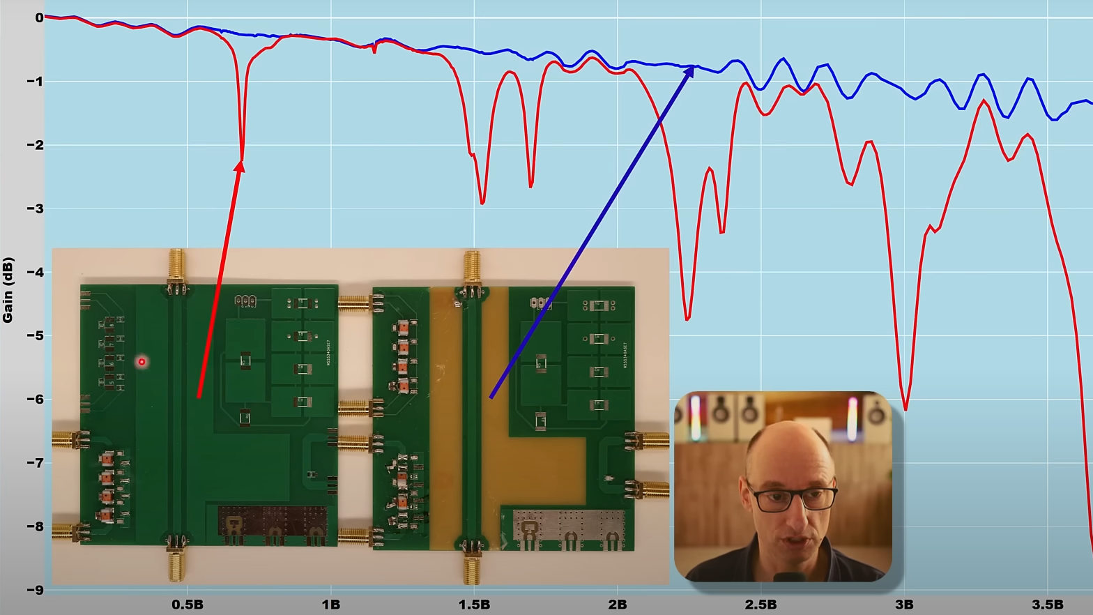
[Hans] shows the effect of interrupting the signal return path on a physical test PCB. The result is pretty bad, with the current forced to detour around the hole in the ground plane. A nanoVNA shows a -20 dB drop at 4 GHz, where the ground plane has effectively become an antenna. Energy will be radiated out, causing signal loss, but worse, it will create an EMC hazard with an unintended transmission.
Additionally, this creates an EMC susceptibility, making the situation worse. Placing a solder blob to bridge the gap directly under the signal trace is all that’s required to make it a continuous straight path again, and the performance is restored.
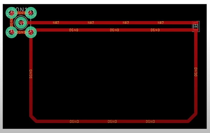
Floating planes are also an issue in RF designs, causing signal resonance and losses. One solution is to pull back the planes near the signal or stitch them to the ground plane with vias placed closely on either side of the signal trace. However, such stitching may slightly affect transmission line impedance and require tweaking the design a little. The next two parts of the series expand on this, hammering home the importance of good ground plane design. These are definitely worth a watch!
PCB design is as much art as science, and we’ve discussed this subject a lot. Here’s our simple guide to rocking RF PCB designs. There’s also a lot of devil in that detail, for example when understanding edge-launch SMA connectors.